Datasheet Details
| Part number | PCF8593 |
|---|---|
| Manufacturer | NXP Semiconductors |
| File Size | 230.83 KB |
| Description | Low-power Clock/Calendar |
| Datasheet |
 PCF8593 Datasheet PCF8593 Datasheet
|
|
|
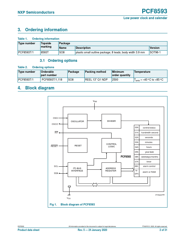
The PCF8593 is a CMOS1 clock and calendar circuit, optimized for low power consumption.
Addresses and data are transferred serially via the two-line bidirectional I2C-bus.
The built-in word address register is incremented automatically after each written or read data byte.
| Part number | PCF8593 |
|---|---|
| Manufacturer | NXP Semiconductors |
| File Size | 230.83 KB |
| Description | Low-power Clock/Calendar |
| Datasheet |
PCF8593 Datasheet
|
|
|
|
Note: Below is a high-fidelity text extraction (approx. 800 characters) for PCF8593. For precise diagrams, and layout, please refer to the original PDF.
PCF8593 Low power clock and calendar Rev. 5 — 24 January 2020 Product data sheet 1. General description The PCF8593 is a CMOS1 clock and calendar circuit, optimized for l...
| Part Number | Description |
|---|---|
| PCF8591 | 8-bit A/D and D/A converter |
| PCF8591P | 8-bit A/D and D/A converter |
| PCF8591T | 8-bit A/D and D/A converter |
| PCF8594C-2 | 256 to 1024 x 8-bit CMOS EEPROMs |
| PCF8598C-2 | 256 to 1024 x 8-bit CMOS EEPROMs |
| PCF85053A | Bootable CPU RTC |
| PCF85063A | Tiny Real-Time Clock/calendar |
| PCF85063ATL | Tiny Real-Time Clock/calendar |
| PCF85063BTL | Tiny Real-Time Clock/calendar |
| PCF85063TP | Tiny Real-Time Clock/calendar |