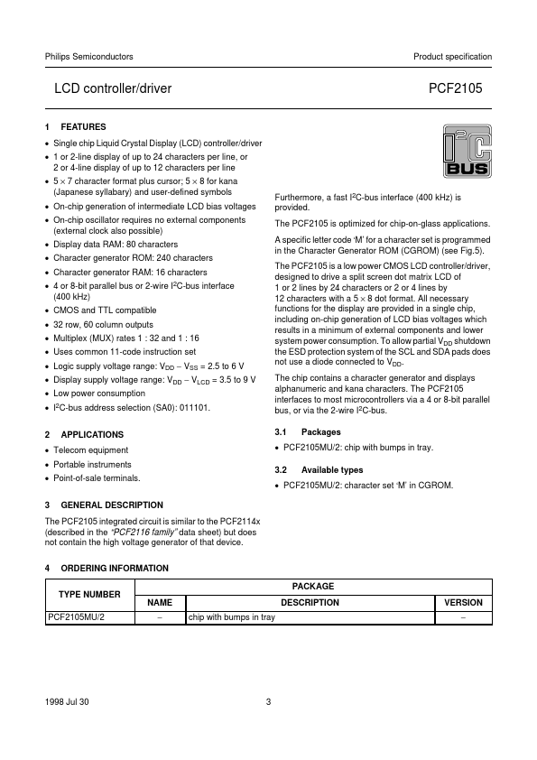
Packages Available types ORDERING INFORMATION BLOCK DIAGRAM PINNING PAD FUNCTIONS RS: Register Select (parallel control) R/W: read/write (parallel control) E: data bus clock (parallel control) DB7 to DB0: data bus (parallel control) C60 to C1: column driver outputs R32 to R1: row driver outputs VLCD
Full PDF Text Transcription for PCF2105 (Reference)
Note: Below is a high-fidelity text extraction (approx. 800 characters) for
PCF2105. For precise diagrams, and layout, please refer to the original PDF.
INTEGRATED CIRCUITS DATA SHEET PCF2105 LCD controller/driver Product specification Supersedes data of 1997 Dec 08 File under Integrated Circuits, IC12 1998 Jul 30 Philips ...
 PCF2105 Datasheet