IRF530N
FEATURES
- ’Trench’ technology
- Low on-state resistance
- Fast switching
- Low thermal resistance
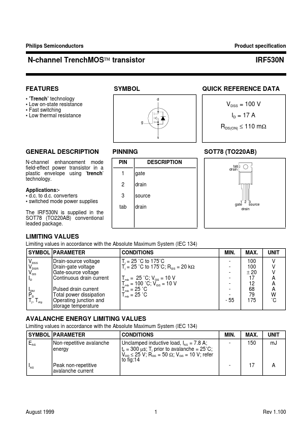
SYMBOL d
QUICK REFERENCE DATA VDSS = 100 V ID = 17 A g
RDS(ON) ≤ 110 mΩ s
GENERAL DESCRIPTION
N-channel enhancement mode field-effect power transistor in a plastic envelope using ’trench’ technology. Applications:- d.c. to d.c. converters
- switched mode power supplies The IRF530N is supplied in the SOT78 (TO220AB) conventional leaded package.
PINNING
PIN 1 2 3 tab gate drain source drain DESCRIPTION
SOT78 (TO220AB) tab drain
1 2 3 gate source drain
LIMITING VALUES
Limiting values in accordance with the Absolute Maximum System (IEC 134) SYMBOL PARAMETER VDSS VDGR VGS ID IDM PD Tj, Tstg Drain-source voltage Drain-gate voltage Gate-source voltage Continuous drain current Pulsed drain current Total power dissipation Operating junction and storage temperature CONDITIONS Tj = 25 ˚C to 175˚C Tj = 25 ˚C to 175˚C; RGS = 20 kΩ Tmb = 25 ˚C; VGS = 10 V Tmb = 100 ˚C; VGS = 10 V Tmb = 25 ˚C...