BUK7505-30A
DESCRIPTION
N-channel enhancement mode standard level field-effect power transistor in a plastic envelope using ’trench’ technology which features very low on-state resistance. It is intended for use in automotive and general purpose switching applications.
QUICK REFERENCE DATA
SYMBOL VDS ID Ptot Tj RDS(ON) PARAMETER Drain-source voltage Drain current (DC) Total power dissipation Junction temperature Drain-source on-state resistance VGS = 10 V MAX. 30 75 230 175 5 UNIT V A W ˚C mΩ
PINNING
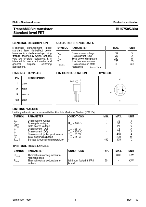
- TO220AB
PIN 1 2 3 tab gate drain DESCRIPTION
PIN CONFIGURATION tab
SYMBOL d g source drain
1 23 s
LIMITING VALUES
Limiting values in accordance with the Absolute Maximum System (IEC 134) SYMBOL VDS VDGR ±VGS ID ID IDM Ptot Tstg, Tj PARAMETER Drain-source voltage Drain-gate voltage Gate-source voltage Drain current (DC) Drain current (DC) Drain current (pulse peak value) Total power dissipation Storage & operating temperature CONDITIONS RGS = 20 kΩ Tmb = 25 ˚C Tmb = 100 ˚C Tmb =...