Datasheet Details
| Part number | 74VHC126 |
|---|---|
| Manufacturer | NXP Semiconductors |
| File Size | 80.02 KB |
| Description | Quad buffer/line driver |
| Datasheet |
 74VHC126 Datasheet 74VHC126 Datasheet
|
|
|
The 74VHC126; 74VHCT126 are high-speed Si-gate CMOS devices and are pin compatible with Low-power Schottky TTL (LSTTL).
They are specified in compliance with JEDEC standard No.
7-A.
| Part number | 74VHC126 |
|---|---|
| Manufacturer | NXP Semiconductors |
| File Size | 80.02 KB |
| Description | Quad buffer/line driver |
| Datasheet |
74VHC126 Datasheet
|
|
|
|
| Brand Logo | Part Number | Description | Manufacturer |
|---|---|---|---|
| 74VHC126 | QUAD BUS BUFFERS | STMicroelectronics | |
| 74VHC126 | Quad buffer/line driver | nexperia | |
| 74VHC126-Q100 | Quad buffer/line driver | nexperia |
| Part Number | Description |
|---|---|
| 74VHC125 | Quad buffer/line driver |
| 74VHC02 | Quad 2-input NOR gate |
| 74VHC02-Q100 | Quad 2-input NOR gate |
| 74VHC08 | Quad 2-input AND gate |
| 74VHC08-Q100 | Quad 2-input AND gate |
| 74VHC541 | Octal buffer/line driver |
| 74VHC541-Q100 | Octal buffer/line driver |
| 74VHCT02 | Quad 2-input NOR gate |
| 74VHCT02-Q100 | Quad 2-input NOR gate |
| 74VHCT08 | Quad 2-input AND gate |
Note: Below is a high-fidelity text extraction (approx. 800 characters) for 74VHC126. For precise diagrams, tables, and layout, please refer to the original PDF.
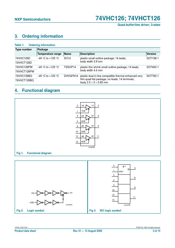
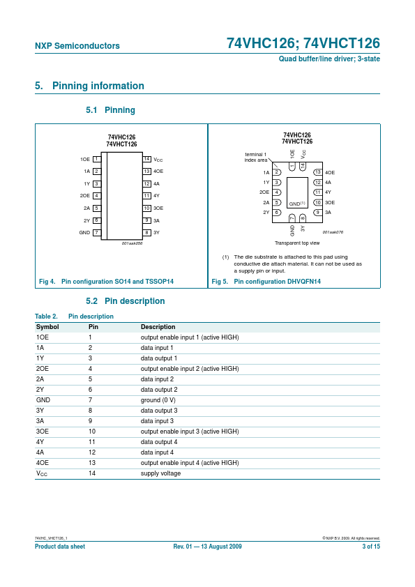
74VHC126; 74VHCT126 Quad buffer/line driver; 3-state Rev. 01 — 13 August 2009 Product data sheet 1. General description The 74VHC126; 74VHCT126 are high-speed Si-gate CMO...