Click to expand full text
74LVC2G66
Bilateral switch
Rev. 01 — 29 June 2004 Product data sheet
1. General description
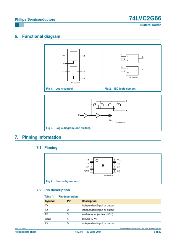
The 74LVC2G66 is a high-performance, low-power, low-voltage, Si-gate CMOS device. The 74LVC2G66 provides two analog switches. Each switch has a input and output (pins Y and Z) and an active HIGH enable input (pin E). When pin E is LOW, the analog switch is turned off.
2. Features
s Wide supply voltage range from 1.65 V to 5.5 V s Very low ON-resistance: x 7.5 Ω (typical) at VCC = 2.7 V x 6.5 Ω (typical) at VCC = 3.3 V x 6 Ω (typical) at VCC = 5 V. s High noise immunity s Complies with JEDEC standard: x JESD8-7 (1.65 V to 1.95 V) x JESD8-5 (2.3 V to 2.7 V) x JESD8-B/JESD36 (2.7 V to 3.6 V). s ESD protection: x HBM EIA/JESD22-A114-B exceeds 2000 V x MM EIA/JESD22-A115-A exceeds 200 V.
 74LVC2G66 Datasheet