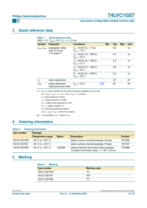
Click to expand full text
www.DataSheet4U.com
74LVC1G57
Low-power configurable multiple function gate
Rev. 01 — 6 September 2004 Product data sheet
1. General description
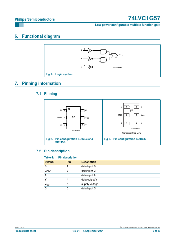
The 74LVC1G57 is a high-performance, low-power, low-voltage, Si-gate CMOS device, superior to most advanced CMOS compatible TTL families. Inputs can be driven from either 3.3 V or 5 V devices. This feature allows the use of this device in a mixed 3.3 V and 5 V environment. This device is fully specified for partial power-down applications using Ioff. The Ioff circuitry disables the output, preventing the damaging backflow current through the device when it is powered down. The 74LVC1G57 provides configurable multiple functions. The output state is determined by eight patterns of 3-bit input.
 74LVC1G57 Datasheet