Datasheet Details
| Part number | 74LVC1G19 |
|---|---|
| Manufacturer | NXP Semiconductors |
| File Size | 83.82 KB |
| Description | 1-of-2 decoder/demultiplexer |
| Datasheet |
 74LVC1G19 Datasheet 74LVC1G19 Datasheet
|
|
|
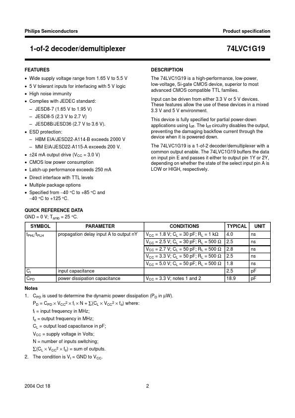
The 74LVC1G19 is a high-performance, low-power, low-voltage, Si-gate CMOS device, superior to most advanced CMOS compatible TTL families.
Input can be driven from either 3.3 V or 5 V devices.
| Part number | 74LVC1G19 |
|---|---|
| Manufacturer | NXP Semiconductors |
| File Size | 83.82 KB |
| Description | 1-of-2 decoder/demultiplexer |
| Datasheet |
74LVC1G19 Datasheet
|
|
|
|
| Part Number | Description | Manufacturer |
|---|---|---|
| 74LVC1G19 | 1-of-2 decoder/demultiplexer | nexperia |
| 74LVC1G19-Q100 | 1-of-2 decoder/demultiplexer | nexperia |
| 74LVC1G10 | SINGLE 3 INPUT POSITIVE NAND GATE | Diodes |
| 74LVC1G10 | Single 3-input NAND gate | nexperia |
| 74LVC1G10-Q100 | Single 3-input NAND gate | nexperia |
| Part Number | Description |
|---|---|
| 74LVC1G11 | Single 3-input AND gate |
| 74LVC1G123 | Single retriggerable monostable multivibrator |
| 74LVC1G126 | Bus buffer/line driver |
| 74LVC1G14 | Single Schmitt-trigger inverter |
| 74LVC1G17 | Single Schmitt-trigger buffer |
The following content is an automatically extracted verbatim text from the original manufacturer datasheet and is provided for reference purposes only.