The following content is an automatically extracted verbatim text
from the original manufacturer datasheet and is provided for reference purposes only.
View original datasheet text
Philips Semiconductors Advanced BiCMOS Products
Product specification
Synchronizing dual D-type flip-flop with metastable immune characteristics
74ABT5074
FEATURES
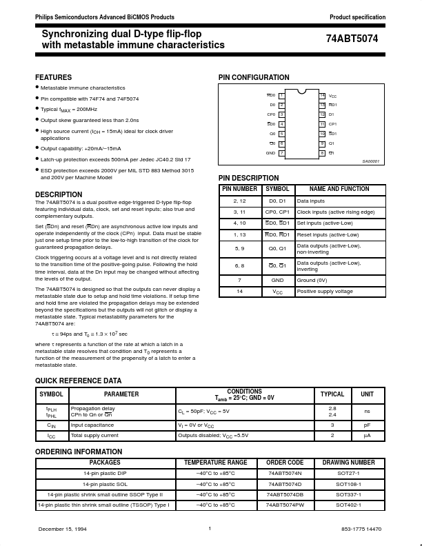
• Metastable immune characteristics • Pin compatible with 74F74 and 74F5074 • Typical fMAX = 200MHz • Output skew guaranteed less than 2.0ns • High source current (IOH = 15mA) ideal for clock driver
applications
PIN CONFIGURATION
RD0 D0 CP0 SD0 Q0 Q0 GND 1 2 3 4 5 6 7 14 13 12 11 10 9 8 VCC RD1 D1 CP1 SD1 Q1 Q1
• Output capability: +20mA/–15mA • Latch-up protection exceeds 500mA per Jedec JC40.
 74ABT5074 Datasheet