NSD1026V Datasheet Text
NSD1026V High Speed, 5A Dual-Channel, Low-Side Gate Driver with Enable
Datasheet (EN) 1.2
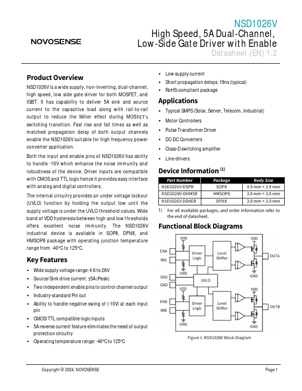
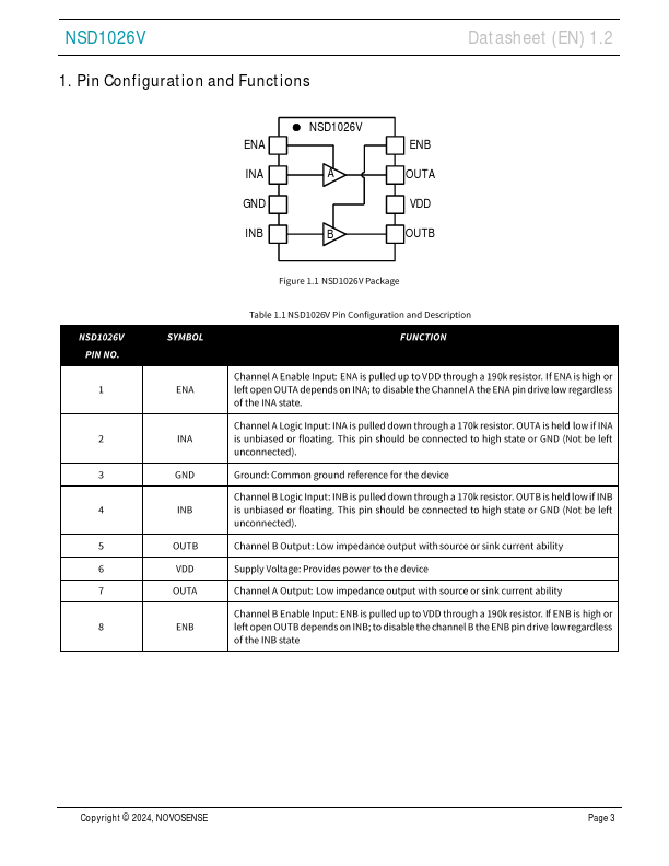
NSD1026V is a wide supply, non-inverting, dual-channel, high speed, low side gate driver for both MOSFET, and IGBT. It has capability to deliver 5A sink and source current to the capacitive load along with rail-to-rail output to reduce the Miller effect during MOS switching transition. Fast rise and fall times as well as matched propagation delay of both output channels enable the NSD1026V suitable for high frequency power converter application.
Both the input and enable pins of NSD1026V has ability to handle -10V which enhance the noise immunity and robustness of the device. Driver inputs are patible with CMOS and TTL logic hence it provides easy interface with analog and digital controllers.
The internal circuitry provides an under voltage lockout (UVLO) function by holding the output low until the supply voltage is under the UVLO threshold values. Wide band of VDD hysteresis between high and low thresholds offers excellent noise immunity. The NSD1026V industrial device is available in SOP8, DFN8, and HMSOP8 package with operating junction temperature range from -40°C to 125°C.
- Low supply current
- Short propagation delays: 19ns (typical)
- RoHS-pliant package
- Typical SMPS (Solar, Server, Tele, Industrial)
- Motor Controllers
- Pulse Transformer Driver
- DC-DC Converters
- Class-D switching amplifier
- Line-drivers
1)
- Wide supply voltage range: 4.6 to 26V
- Source/Sink drive current: ±5A (Peak)
- Two independent enable pins to control channel output
- Industry-standard Pin out
- Ability to handle negative swing of (-10V) at each input pin
- CMOS/TTL patible logic inputs
- 5A reverse current feature eliminates the need of output protection circuitry
-...