Click to expand full text
NIKO-SEM
P-Channel Logic Level Enhancement
Mode Field Effect Transistor
P06P03LCG
SOT-89 Lead-Free
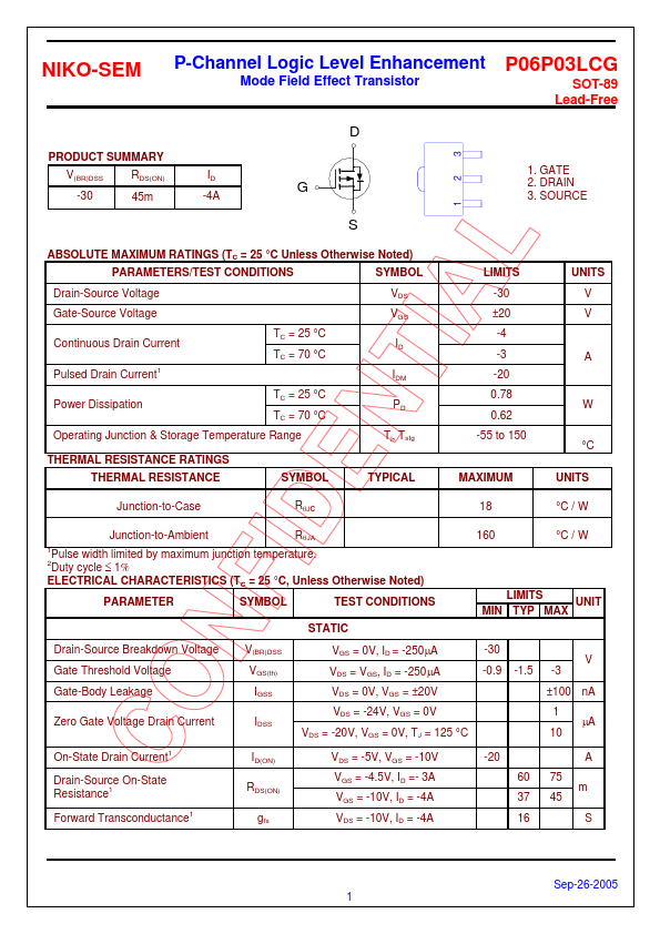
D
PRODUCT SUMMARY V(BR)DSS -30 RDS(ON) 45m ID -4A
3
G S
1
1. GATE 2. DRAIN 3. SOURCE
ABSOLUTE MAXIMUM RATINGS (TC = 25 °C Unless Otherwise Noted) PARAMETERS/TEST CONDITIONS Drain-Source Voltage Gate-Source Voltage Continuous Drain Current Pulsed Drain Current Power Dissipation
1
SYMBOL VDS VGS
2
LIMITS -30 ±20 -4 -3 -20 0.78 0.62 -55 to 150
UNITS V V
TC = 25 °C TC = 70 °C
ID IDM
A
TC = 25 °C TC = 70 °C
PD Tj, Tstg
W
Operating Junction & Storage Temperature Range THERMAL RESISTANCE RATINGS THERMAL RESISTANCE Junction-to-Case Junction-to-Ambient
1 2
°C UNITS °C / W °C / W
SYMBOL RθJc RθJA
TYPICAL
MAXIMUM 18 160
Pulse width limited by maximum junction temperature.
 P06P03LCG Datasheet