NCE1512I
Description
The NCE1512I uses advanced trench technology and design to provide excellent RDS(ON) with low gate charge. It can be used in a wide variety of applications.
General Features
- VDS = 150V,ID =12A RDS(ON) <160mΩ @ VGS=10V (Typ:130mΩ)
- High density cell design for ultra low Rdson
- Fully characterized avalanche voltage and current
- Excellent package for good heat dissipation
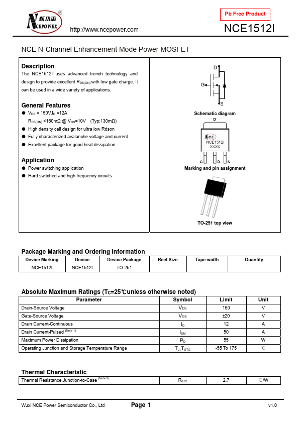
S Schematic diagram
Application
- Power switching application
- Hard switched and high frequency circuits
Marking and pin assignment
TO-251 top view
Package Marking and Ordering Information
Device Marking
Device
Device Package
TO-251
Reel Size
- Tape width
- Quantity
- Absolute Maximum Ratings (TC=25℃unless otherwise noted)
Parameter
Symbol
Drain-Source Voltage
Gate-Source Voltage
Drain Current-Continuous Drain Current-Pulsed (Note 1)
ID IDM
Maximum Power Dissipation
Operating Junction and Storage Temperature Range
TJ,TSTG
Limit
150 ±20 12 50...