Datasheet Details
| Part number | NT5SV4M16DT |
|---|---|
| Manufacturer | NANYA |
| File Size | 258.66 KB |
| Description | (NT5SVxxMxxDT) 64Mb Synchronous DRAM |
| Datasheet |
 NT5SV4M16DT Datasheet NT5SV4M16DT Datasheet
|
|
|
Download the NT5SV4M16DT datasheet PDF. This datasheet also covers the NT5SV16M4DT variant, as both devices belong to the same (nt5svxxmxxdt) 64mb synchronous dram family and are provided as variant models within a single manufacturer datasheet.
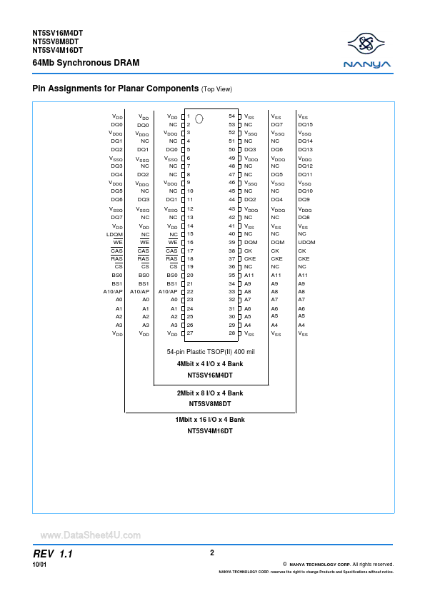
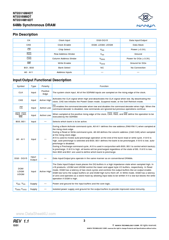
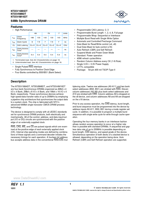
The NT5SV16M4DT, NT5SV8M8DT, and NT5SV4M16DT are four-bank Synchronous DRAMs organized as 4Mbit x 4 I/O x 4 Bank, 2Mbit x 8 I/O x 4 Bank, and 1Mbit x 16 I/O x 4 Bank, respectively.
| Part number | NT5SV4M16DT |
|---|---|
| Manufacturer | NANYA |
| File Size | 258.66 KB |
| Description | (NT5SVxxMxxDT) 64Mb Synchronous DRAM |
| Datasheet |
NT5SV4M16DT Datasheet
|
|
|
|
| Part Number | Description | Manufacturer |
|---|---|---|
| NT5SV16M16BS | (NT5SVxxMxxBx) 256Mb SDRAM | Nanya Technology |
| NT5SV16M16BT | (NT5SVxxMxxBx) 256Mb SDRAM | Nanya Technology |
| NT5SV16M8CT | (NT5SVxxMxxCT) 128Mb SDRAM | Nanya Techology |
| NT5SV32M6CT | (NT5SVxxMxxCT) 128Mb SDRAM | Nanya Techology |
| NT5SV32M8BS | (NT5SVxxMxxBx) 256Mb SDRAM | Nanya Technology |
| Part Number | Description |
|---|---|
| NT5SV16M16AT | (NT5SVxxMxxAT) Synchronous DRAM |
| NT5SV16M4DT | (NT5SVxxMxxDT) 64Mb Synchronous DRAM |
| NT5SV32M8AT | (NT5SVxxMxxAT) Synchronous DRAM |
| NT5SV64M4AT | (NT5SVxxMxxAT) Synchronous DRAM |
| NT5SV8M16FS | 128Mb Synchronous DRAM |