Download the S12VREGV1 datasheet PDF.
This datasheet also covers the S12 variant, as both devices belong to the same mc9s12dt128 device user guide v02.09 family and are provided as variant models within a single manufacturer datasheet.
Description
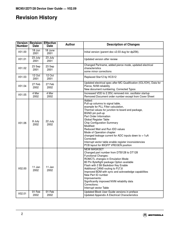
Initial version (parent doc v2.03 dug for dp256).
Features
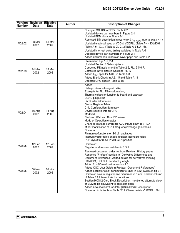
- Corrected KWP5 pin name in Fig 2-1 112LQFP pin assignments Corrected pull resistor CTRL/reset states for PE7 and PE4-PE0 in Table 2.1 “Signal Properties” Mentioned “S12LRAE” bootloader in Flash section 17 Corrected footnote on clamp of TEST pin under Table A-1 “Absolute Maximum Ratings” Corrected minimum bus frequency to 0.25MHz in Table A-4 “Operating Conditions” Replaced “burst programming” by “row programming” in A.3 “NVM, Flash and EEPROM” Corrected blank check time for EEPROM in Table A-11.
 S12VREGV1 Datasheet