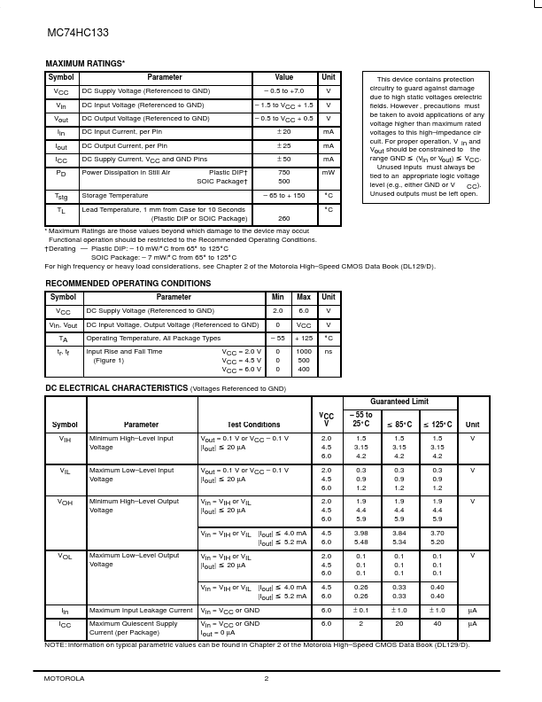
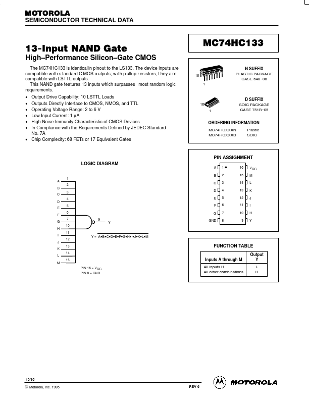
13 inputs which surpasses most random logic requirements.
Output Drive Capability: 10 LSTTL Loads Outputs Directly Interface to CMOS, NMOS, and TTL Operating Voltage Range: 2 to 6 V Low Input Current: 1 µA High Noise Immunity Characteristic of CMOS Devices In Compliance with the Requirements Defined by JEDEC Standard No. 7A.
Chip Complexity: 68 FETs or 17 Equivalent Gates
16
MC74HC133
N SUFFIX.
Full PDF Text Transcription for MC74HC133 (Reference)
Note: Below is a high-fidelity text extraction (approx. 800 characters) for
MC74HC133. For precise diagrams, and layout, please refer to the original PDF.
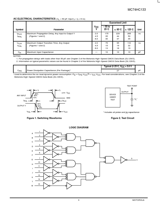
MOTOROLA SEMICONDUCTOR TECHNICAL DATA 13-Input NAND Gate High–Performance Silicon–Gate CMOS The MC74HC133 is identical in pinout to the LS133. The device inputs are compa...
View more extracted text
HC133 is identical in pinout to the LS133. The device inputs are compatible w ith s tandard C MOS o utputs; w ith p ullup r esistors, t hey a re compatible with LSTTL outputs. This NAND gate features 13 inputs which surpasses most random logic requirements. • • • • • • Output Drive Capability: 10 LSTTL Loads Outputs Directly Interface to CMOS, NMOS, and TTL Operating Voltage Range: 2 to 6 V Low Input Current: 1 µA High Noise Immunity Characteristic of CMOS Devices In Compliance with the Requirements Defined by JEDEC Standard No.
More Datasheets from Motorola Semiconductor (now NXP Semiconductors)
 MC74HC133 Datasheet