Datasheet Details
| Part number | J271 |
|---|---|
| Manufacturer | Motorola Semiconductor (now NXP Semiconductors) |
| File Size | 26.70 KB |
| Description | JFET CHOPPER TRANSISTOR |
| Datasheet |
 J271 Datasheet J271 Datasheet
|
|
|
|
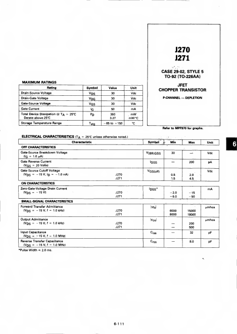
Download the J271 datasheet PDF. This datasheet also covers the J270 variant, as both devices belong to the same jfet chopper transistor family and are provided as variant models within a single manufacturer datasheet.
| Part number | J271 |
|---|---|
| Manufacturer | Motorola Semiconductor (now NXP Semiconductors) |
| File Size | 26.70 KB |
| Description | JFET CHOPPER TRANSISTOR |
| Datasheet |
J271 Datasheet
|
|
|
|
| Part Number | Description | Manufacturer |
|---|---|---|
| J271 | P-Channel JFET | Calogic LLC |
| J271 | P-Channel JFET | InterFET |
| J271 | (J270 / J271) P-Channel JFETs | Vishay Siliconix |
| J271 | P-Channel Switch | Fairchild Semiconductor |
| J270 | P-Channel JFET | Calogic LLC |
| Part Number | Description |
|---|---|
| J270 | JFET CHOPPER TRANSISTOR |
The following content is an automatically extracted verbatim text from the original manufacturer datasheet and is provided for reference purposes only.