The following content is an automatically extracted verbatim text
from the original manufacturer datasheet and is provided for reference purposes only.
View original datasheet text
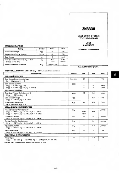
2N3330
MAXIMUM RATINGS
Rating Drain-Gate Voltage Reverse Gate-Source Voltage Gate Current Total Device Dissipation (d T/ = 25°C
Derate above 25°C Storage Temperature Range
Symbol VDG vgsr
•g
Pd
Tstg
Value 20 20 10 0.3 2.0
- 65 to + 200
Unit Vdc Vdc
mAdc
Watts mW/°C
°C
ELECTRICAL CHARACTERISTICS (TA = 25°C unless otherwise noted.)
Characteristic
OFF CHARACTERISTICS
Gate-Source Breakdown Voltage (Iq = 10 /iAdc, V DS = 0)
Gate Reverse Current
(VGS = 10 Vdc, V DS = 0) (VGS = 10 Vdc, Vqs = 0, Ta = 150°C) ON CHARACTERISTICS
Zero-Gate- Voltage Drain Current! 1)
(VDS = -10Vdc,VG S = 0)
Gate-Source Voltage
( V DG = -15 Vdc, Iq = 10/iAdc)
Drain-Source Resistance
(Iq = 100 /iAdc, Vqs = 0)
SMALL-SIGNAL CHARACTERISTICS
Forward Transfer Admittance(l) (VdS = - 10 Vdc, Id = 2.0 mAdc, f = 1.
 2N3330 Datasheet