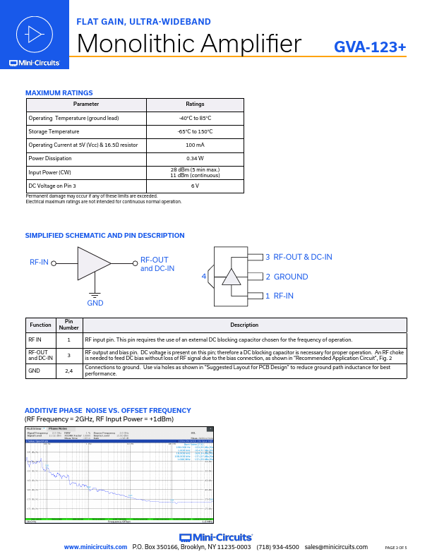
Description
RF-IN
RF-OUT and DC-IN
4
3 RF-OUT & DC-IN 2 GROUND
GND
1 RF-IN
Function
Pin Number
Description
RF IN
1
RF input pin.This pin requires the use of an external DC blocking capacitor chosen for the frequency of operation.RF-OUT and DC-IN
3
RF output and bias pin.DC voltage is present on this pin; therefore a DC blocking capacitor is necessary for proper operation.An RF choke is needed to feed DC bias without loss of RF signal due to the bias connection, as shown in “Recommended App
Features
- Feature
Ultra Broad Band: 0.01 to 12 GHz
Ultra Flat Gain ±0.7 dB typ: 0.05 - 8 GHz
Low additive phase noise
No External Matching Components Required Excellent ESD HBM: class 1C (1000 to.
 GVA-123+ Datasheet