Datasheet4U Logo Datasheet4U.com

ZL40260 - Low Additive Jitter 2 x10 LVPECL Fanout Buffer

Description

6 Functional Description 8 Clock Inputs 8 Clock Outputs 11 Termination of unused inputs and outputs 13 Power Consumption 13 Power Supply Filtering 13 Power Supplies and Power-up Sequence 13 AC and DC Electrical Characteristics 13 Absolute Maximum Ratings 14 Recommended Operating Conditions 14 D

Features

  • Two inputs accept any differential (LVPECL, HCSL, LVDS, SSTL, CML) or single ended LVCMOS signal.
  • Ten 2.5V/3.3V LVPECL outputs.
  • Ultra-low additive jitter: 53fs for 125 MHz clock measured in 12KHz to 20MHz band.
  • Supports clock frequencies from 0 to 1.6GHz.
  • Supports 2.5V or 3.3V power supplies.
  • Embedded Low Drop Out (LDO) Voltage regulator provides superior Power Supply Noise Rejection.
  • Maximum output to output skew of 50ps.
  • Maximum input to output delay of.

📥 Download Datasheet

Full PDF Text Transcription

Click to expand full text
Data Sheet ZL40260 
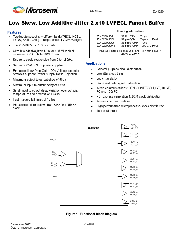
Low Skew, Low Additive Jitter 2 x10 LVPECL Fanout Buffer Features  Two inputs accept any differential (LVPECL, HCSL, LVDS, SSTL, CML) or single ended LVCMOS signal  Ten 2.5V/3.3V LVPECL outputs  Ultra-low additive jitter: 53fs for 125 MHz clock measured in 12KHz to 20MHz band  Supports clock frequencies from 0 to 1.6GHz  Supports 2.5V or 3.3V power supplies  Embedded Low Drop Out (LDO) Voltage regulator provides superior Power Supply Noise Rejection  Maximum output to output skew of 50ps  Maximum input to output delay of 1.2ns  Small input to output delay variation over voltage, temperature and process of 0.
Published: |