Datasheet4U Logo Datasheet4U.com

PIC14000 - 28-Pin Programmable Mixed Signal Controller

Download the PIC14000 datasheet PDF. This datasheet also covers the PIC variant, as both devices belong to the same 28-pin programmable mixed signal controller family and are provided as variant models within a single manufacturer datasheet.

Description

3 2.0: Device Varieties 5 3.0: Architectural Overview 7 4.0: Memory Organization 13 5.0: I/O Ports 25 6.0: Timer Modules 37 7.0: Inter-integrated Circuit Serial Port (I2C™) 41 8.0: Analog Modules for A/D Conversion 57 9.0: Other Analog Modules 65 10.0: Special

Features

  • Slope Analog-to-Digital (A/D) converter - Eight external input channels including two channels with selectable level shift inputs - Six internal input channels - 16-bit programmable timer with capture register - 16 ms maximum conversion time at maximum (16-bit) resolution and 4 MHz clock - 4-bit programmable current source.
  • Internal bandgap voltage reference.
  • Factory calibrated with calibration constants stored in EPROM.
  • On-chip temperature sensor.

📥 Download Datasheet

Note: The manufacturer provides a single datasheet file (PIC-140.pdf) that lists specifications for multiple related part numbers.

Datasheet Details

Part number PIC14000
Manufacturer Microchip
File Size 953.49 KB
Description 28-Pin Programmable Mixed Signal Controller
Datasheet download datasheet PIC14000 Datasheet

Full PDF Text Transcription

Click to expand full text
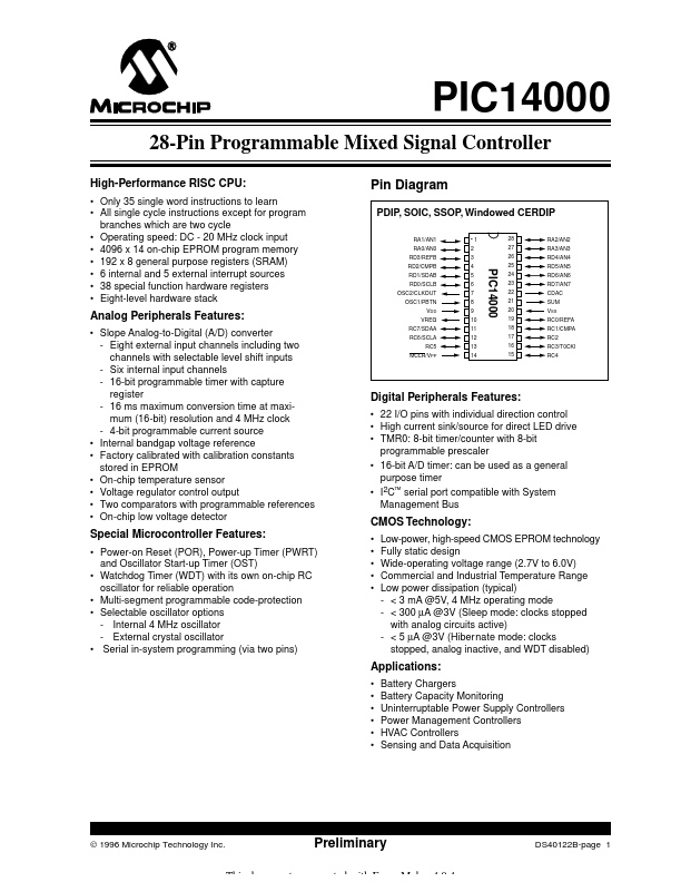
PIC14000 28-Pin Programmable Mixed Signal Controller High-Performance RISC CPU: • Only 35 single word instructions to learn • All single cycle instructions except for program branches which are two cycle • Operating speed: DC - 20 MHz clock input • 4096 x 14 on-chip EPROM program memory • 192 x 8 general purpose registers (SRAM) • 6 internal and 5 external interrupt sources • 38 special function hardware registers • Eight-level hardware stack Pin Diagram PDIP, SOIC, SSOP, Windowed CERDIP RA1/AN1 RA0/AN0 RD3/REFB RD2/CMPB RD1/SDAB RD0/SCLB OSC2/CLKOUT OSC1/PBTN VDD VREG RC7/SDAA RC6/SCLA RC5 MCLR/VPP •1 2 3 4 5 6 7 8 9 10 11 12 13 14 28 27 26 25 RA2/AN2 RA3/AN3 RD4/AN4 RD5/AN5 RD6/AN6 RD7/AN7 CDAC SUM VSS RC0/REFA RC1/CMPA RC2 RC3/T0CKI RC4 PIC14000 24 23 22 21 20 19 18 17 16 15 Analog
Published: |