Datasheet Details
| Part number | P2S28D40CTP |
|---|---|
| Manufacturer | MIRA |
| File Size | 301.58 KB |
| Description | (P2S28D30CTP / P2S28D40CTP) 128M Double Data Rate Synchronous DRAM |
| Datasheet |
 P2S28D40CTP Datasheet P2S28D40CTP Datasheet
|
|
|
This page provides the datasheet information for the P2S28D40CTP, a member of the P2S28D30CTP (P2S28D30CTP / P2S28D40CTP) 128M Double Data Rate Synchronous DRAM family.
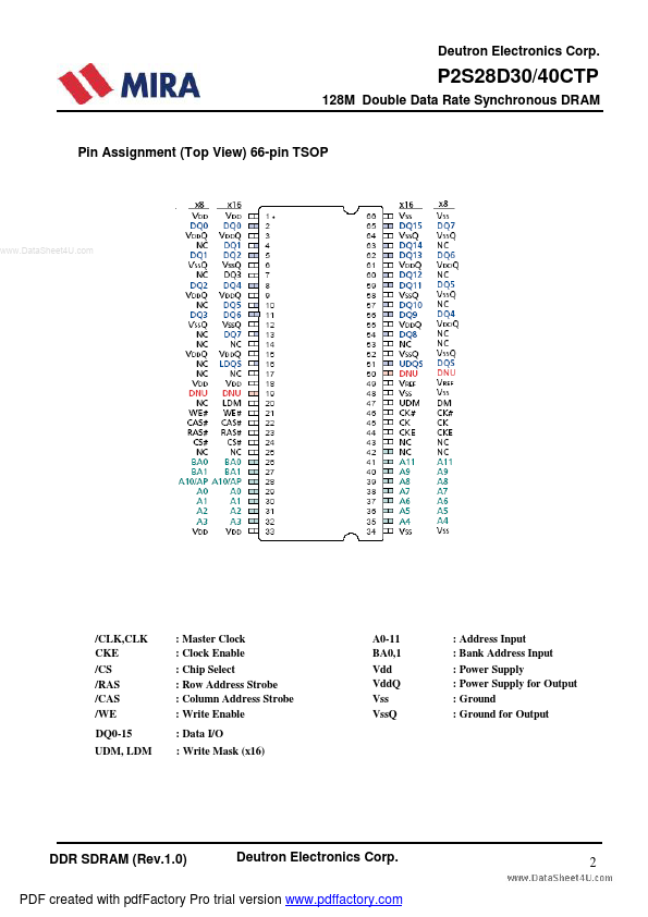
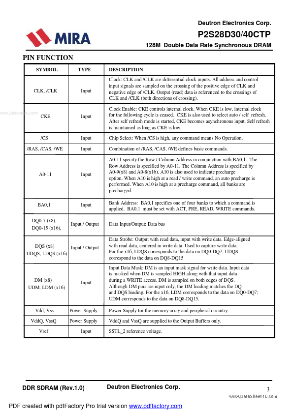
P2S28D30CTP is a 4-bank x 4,194,304-word x 8bit,P2S28D40CTP is a 4-bank x 2,097,152-word x 16bit double data rate synchronous DRAM , with SSTL_2 interface.
All control and address signals www.DataSheet4U.com are referenced to the rising edge of CLK.
| Part number | P2S28D40CTP |
|---|---|
| Manufacturer | MIRA |
| File Size | 301.58 KB |
| Description | (P2S28D30CTP / P2S28D40CTP) 128M Double Data Rate Synchronous DRAM |
| Datasheet |
P2S28D40CTP Datasheet
|
|
|
|