Datasheet Details
| Part number | LSK170D |
|---|---|
| Manufacturer | LINEAR SYSTEMS |
| File Size | 1.14 MB |
| Description | Single N-Channel JFET |
| Datasheet |
 LSK170D Datasheet LSK170D Datasheet
|
|
|
Download the LSK170D datasheet PDF. This datasheet also covers the LSK170 variant, as both devices belong to the same single n-channel jfet family and are provided as variant models within a single manufacturer datasheet.
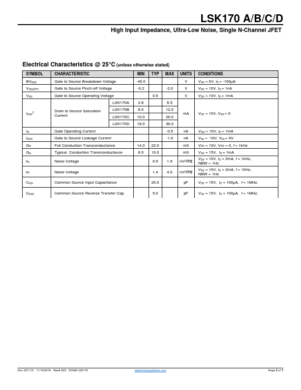
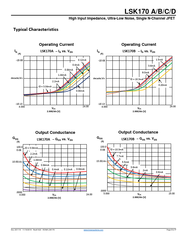
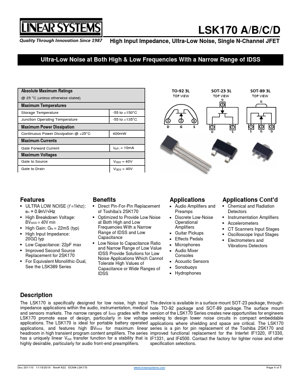
The LSK170 is specifically designed for low noise, high input The device is available in a surface mount SOT-23 package, throughimpedance applications within the audio, instrumentation, medical hole TO-92 package and SOT-89 package.
The surface mount and sensors markets.
| Part number | LSK170D |
|---|---|
| Manufacturer | LINEAR SYSTEMS |
| File Size | 1.14 MB |
| Description | Single N-Channel JFET |
| Datasheet |
LSK170D Datasheet
|
|
|
|
| Part Number | Description | Manufacturer |
|---|---|---|
| LSK170A | Ultra Low Noise | Micross |
| Part Number | Description |
|---|---|
| LSK170 | Single N-Channel JFET |
| LSK170A | Single N-Channel JFET |
| LSK170B | Single N-Channel JFET |
| LSK170C | Single N-Channel JFET |
| LSK389 | Ultra Low Noise Monolithic Dual N-Channel JFET Amplifier |
| LSK389A | Ultra Low Noise Monolithic Dual N-Channel JFET Amplifier |
| LSK389B | Ultra Low Noise Monolithic Dual N-Channel JFET Amplifier |
| LSK389C | Ultra Low Noise Monolithic Dual N-Channel JFET Amplifier |
| LSK389D | Ultra Low Noise Monolithic Dual N-Channel JFET Amplifier |
| LSK489 | DUAL N-CHANNEL JFET AMPLIFIER |
The following content is an automatically extracted verbatim text from the original manufacturer datasheet and is provided for reference purposes only.