The following content is an automatically extracted verbatim text
from the original manufacturer datasheet and is provided for reference purposes only.
View original datasheet text
SMD Type
MOSFET
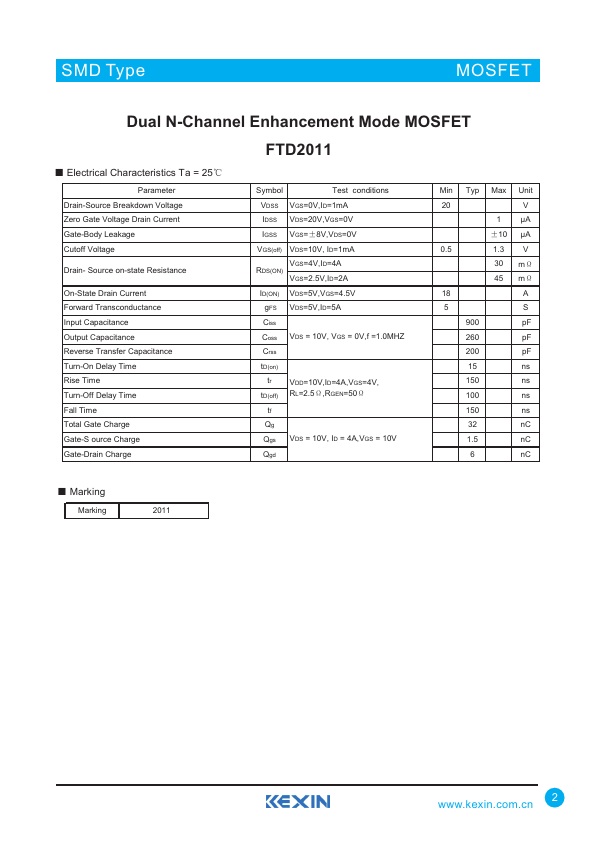
Dual N-Channel Enhancement Mode MOSFET FTD2011
■ Features
● RDS(ON)=30mΩ Max. @VGS=4V ● RDS(ON)=45mΩ Max. @VGS=2.5V
D1 S1 S1 G1
TSSOP-8
Unit: mm
1 : Drain1
2 : Source1
3 : Source1
4 : Gate1
5 : Gate2
6 : Source2
D2
7 : Source2
S2
8 : Drain2
S2
G2
■ Absolute Maximum Ratings Ta = 25℃
Parameter
Drain-Source Voltage
Gate-Source Voltage
Drain-Current
-Continuous
-Pulsed
(NOTE 1)
Power Dissipation
(NOTE 2)
Thermal Resistance,Junction- to-Ambient
Operating Junction and Storage Temperature Range
Note: 1. PW≤10μs, duty cycle≤1% 2. Mounted on a ceramic board (1000mm2×0.8mm)
Symbol VDS VGS ID IDM PD RθJA
Tj.Tstg
Rating 20
±10 5 20 1.3 96
-55 to 150
Unit V V A A W
℃/W ℃
1 www.kexin.com.

 FTD2011 Datasheet