RDS(ON) < 0.5Ω (VGS = 2.5V)
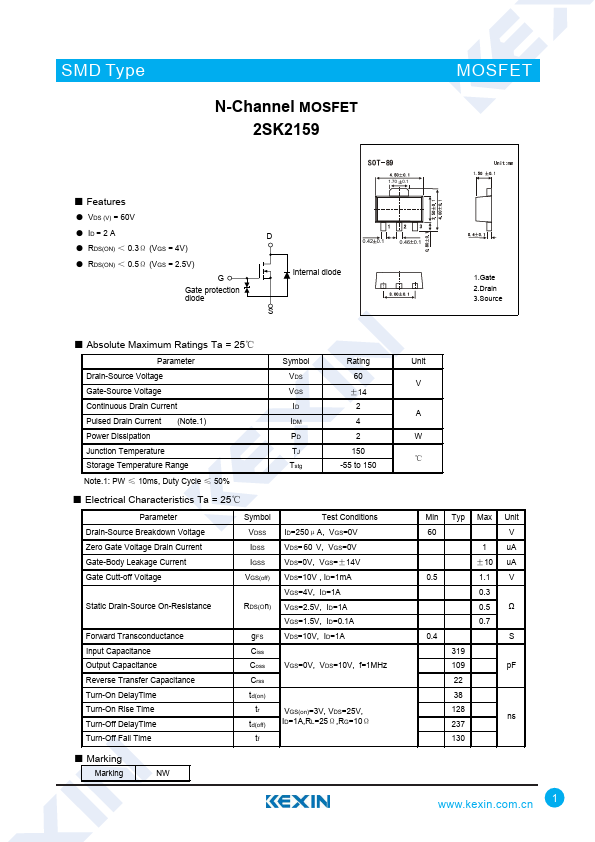
G Gate protection diode
1.70 0.1
D
0.42 0.1
0.46 0.1
Internal diode
S
1.Gate 2.Drain 3.Source.
Absolute Maximum Ratings Ta = 25℃
Parameter Drain-Source Voltage Gate-Source Voltage Continuous Drain Current Pulsed Drain Current (Note.1) Power Dissipation Junction Temperature Storage Temperature Range
Symbol VDS VGS ID IDM PD TJ Tstg
Rating 60
±14 2 4 2
150 -55 to 150
Note.1: PW ≤.
The following content is an automatically extracted verbatim text
from the original manufacturer datasheet and is provided for reference purposes only.
View original datasheet text
SMD Type
N-Channel MOSFET 2SK2159
MOSFET
■ Features
● VDS (V) = 60V ● ID = 2 A ● RDS(ON) < 0.3Ω (VGS = 4V) ● RDS(ON) < 0.5Ω (VGS = 2.5V)
G Gate protection diode
1.70 0.1
D
0.42 0.1
0.46 0.1
Internal diode
S
1.Gate 2.Drain 3.Source
■ Absolute Maximum Ratings Ta = 25℃
Parameter Drain-Source Voltage Gate-Source Voltage Continuous Drain Current Pulsed Drain Current (Note.1) Power Dissipation Junction Temperature Storage Temperature Range
Symbol VDS VGS ID IDM PD TJ Tstg
Rating 60
±14 2 4 2
150 -55 to 150
Note.
 2SK2159 Datasheet