KMB050N60PA
Description
It s mainly suitable for low viltage applications such as automotive, DC/DC converters and a load switch in battery powered applications
N CHANNEL MOS FIELD EFFECT TRANSISTOR
O C F G B Q
DIM MILLIMETERS _ 0.2 9.9 + A B C D E
FEATURES
VDSS= 60V, ID= 50A Drain-Source ON Resistance : RDS(ON)=18m (Max.) @VGS = 10V
D I K M L
I J K L M N O
15.95 MAX 1.3+0.1/-0.05 _ 0.1 0.8 + _ 0.2 3.6 + _ 0.1 2.8 + 3.7 0.5+0.1/-0.05 1.5 _ 0.3 13.08 + 1.46 _ 0.1 1.4 + _ 0.1 1.27 + _ 0.2 2.54 + _ 0.2 4.5 + _ 0.2 2.4 + _ 0.2 9.2 +
MOSFET MAXIMUM RATING (Ta=25
CHARACTERISTIC Drain-Source Voltage Gate-Source Voltage DC Drain Current Pulsed (Note 1) Drain-Source Diode Forward Current Drain Power Dissipation Maximum Junction Temperature Storage Temperature Range Note1) Pulse Test : Pulse width IDP IS
Unless otherwise noted)
RATING 60 25 50 200 50 120 -55 175 -55 175 1% UNIT V V A A A W
SYMBOL VDSS VGSS I D-
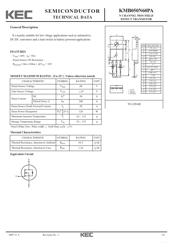
1. GATE 2. DRAIN 3. SOURCE
TO-220AB...