Full PDF Text Transcription for KIC7SZ38FU (Reference)
Note: Below is a high-fidelity text extraction (approx. 800 characters) for
KIC7SZ38FU. For precise diagrams, and layout, please refer to the original PDF.
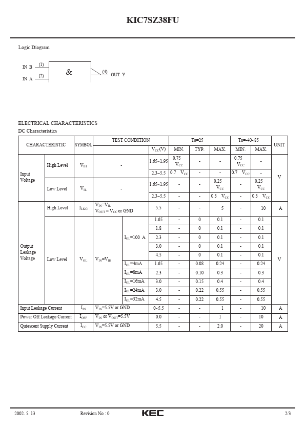
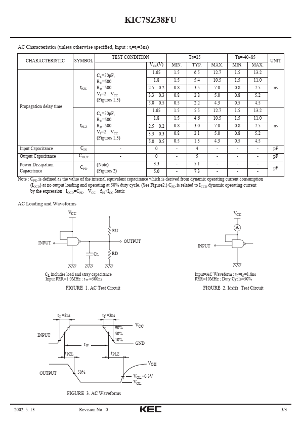
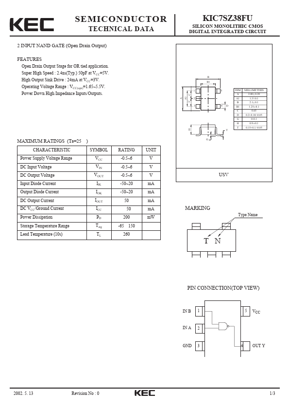
SEMICONDUCTOR TECHNICAL DATA 2 INPUT NAND GATE (Open Drain Output) FEATURES Open Drain Output Stage for OR tied application. Super High Speed : 2.4ns(Typ.) 50pF at VCC=5V...
View more extracted text
for OR tied application. Super High Speed : 2.4ns(Typ.) 50pF at VCC=5V. High Output Sink Drive : 24mA at VCC=3V. Operating Voltage Range : VCC(opr)=1.65~5.5V. Power Down High Impedance Inputs/Outputs. MAXIMUM RATINGS (Ta=25 ) CHARACTERISTIC SYMBOL Power Supply Voltage Range DC Input Voltage DC Output Voltage Input Diode Current Output Diode Current DC Output Current DC VCC/Ground Current Power Dissipation Storage Temperature Range VCC VIN VOUT IIK IOK IOUT ICC PD Tstg Lead Temperature (10s) TL RATING -0.5~6 -0.5~6 -0.
 KIC7SZ38FU Datasheet