Datasheet4U Logo Datasheet4U.com

22346WMVEP - Quad Digitally Controlled Potentiometers

Description

TSSOP PIN 1 2 3 4 5 6 7 8 9 10 11 12 13 14 15 16 17 18 19 20 SYMBOL RH3 RL3 RW3 A2 SCL SDA GND RW2 RL2 RH2 RW1 RL1 RH1 A0 A1 VCC SHDN RH0 RL0 RW0 GND DESCRIPTION “High” terminal of DCP3 “Low” terminal of DCP3 “Wiper” terminal of DCP3 Device address input for the I2C interface Open drain I2C inter

Features

  • Specifications per DSCC VID V62/08605-01XE.
  • Full Mil-Temp Electrical Performance from -55°C to +125°C.
  • Controlled Baseline with One Wafer Fabrication Site and One Assembly/Test Site.
  • Full Homogeneous Lot Processing in Wafer Fab.
  • No Combination of Wafer Fabrication Lots in Assembly.
  • Full Traceability Through Assembly and Test by Date/Trace Code Assignment.
  • Enhanced Process Change Notification.
  • Enhanced Obsolescence Managemen.

📥 Download Datasheet

Full PDF Text Transcription

Click to expand full text
DATASHEET ISL22346WM Quad Digitally Controlled Potentiometers (XDCP™) Low Noise, Low Power I2C Bus, 128 Taps FN6624 Rev 1.00 November 11, 2011 
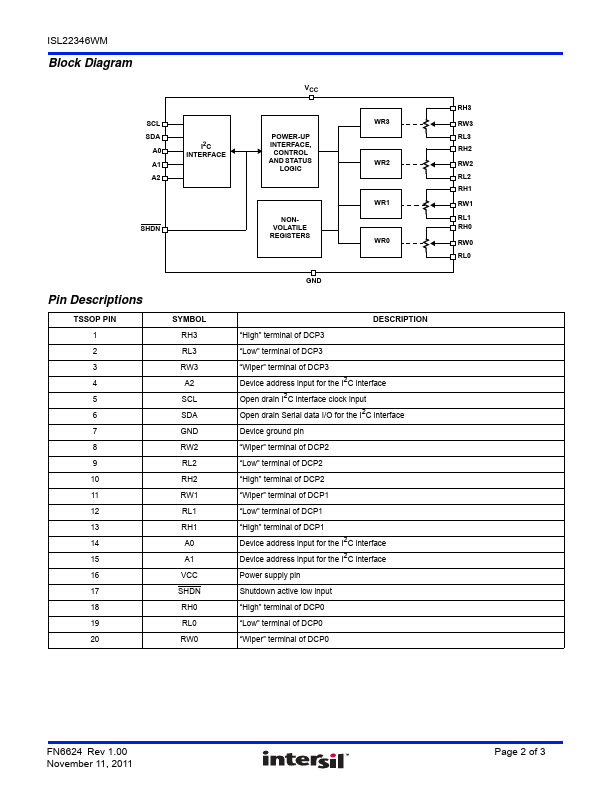
The ISL22346WMVEP integrates four digitally controlled potentiometers (DCP) and non-volatile memory on a monolithic CMOS integrated circuit. The digitally controlled potentiometers are implemented with a combination of resistor elements and CMOS switches. The position of the wipers are controlled by the user through the I2C bus interface. Each potentiometer has an associated volatile Wiper Register (WR) and a non-volatile Initial Value Register (IVR) that can be directly written to and read by the user. The contents of the WR controls the position of the wiper.
Published: |