Click to expand full text
HSP9501
Data Sheet January 1999 File Number
2786.4
Programmable Data Buffer
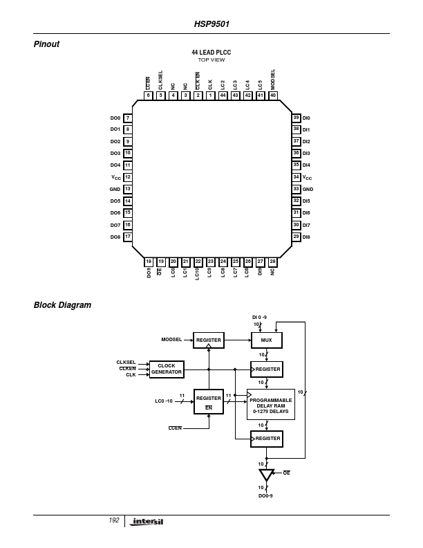
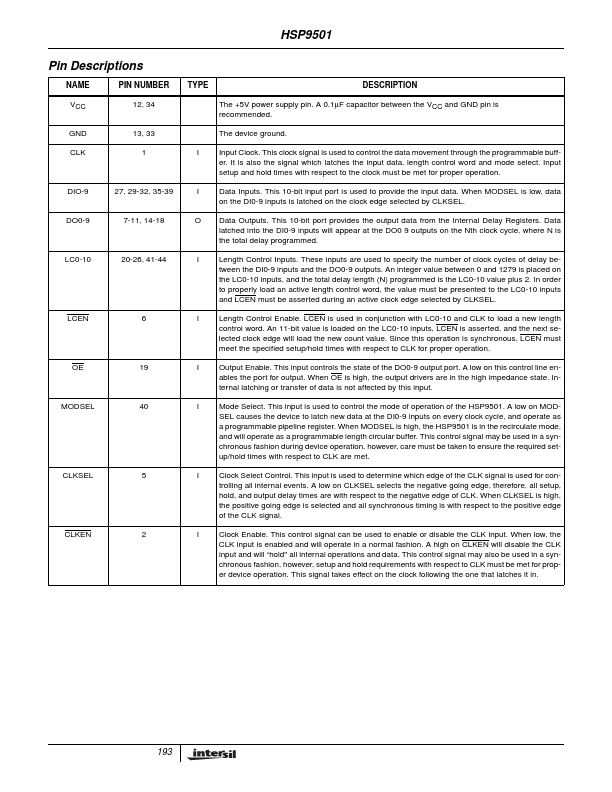
The HSP9501 is a 10-Bit wide programmable data buffer designed for use in high speed digital systems. Two different modes of operation can be selected through the use of the MODSEL input. In the delay mode, a programmable data pipeline is created which can provide 2 to 1281 clock cycles of delay between the input and output data. In the data recirculate mode, the output data path is internally routed back to the input to provide a programmable circular buffer. The length of the buffer or amount of delay is programmed through the use of the 11-bit Length Control Input Port (LC010) and the Length Control Enable (LCEN).
 HSP9501 Datasheet