Description
COMP (Pin 7) and FB (Pin 8)
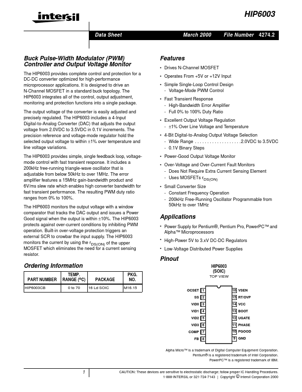
OCSET 1 SS 2 VID0 3 VID1 4 VID2 5 VID3 6 COMP 7 FB 8 16 VSEN 15 RT/OVP 14 VCC 13 BOOT 12 UGATE 11 PHASE 10 PGOOD 9 GND
COMP and FB are the available external pins of the error amplifier.The FB pin is the inverting input of the error amplifier and the COMP pin is the error amplifier output.These pins are used to compensate the voltage-control feedback loop of the converter.GND (Pin 9)
Signal ground for the IC.All voltage levels are measured with respect to this pin.
Features
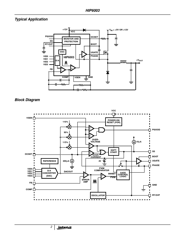
- a 15MHz gain-bandwidth product and 6V/ms slew rate which enables high converter bandwidth for fast transient performance. The resulting PWM duty ratio ranges from 0% to 100%. The HIP6003 monitors the output voltage with a window comparator that tracks the DAC output and issues a Power Good signal when the output is within ±10%. The HIP6003 protects against over-current conditions by inhibiting PWM operation. Built-in over-voltage protection triggers an external SCR to crowbar the input supply. T.
 HIP6003 Datasheet