CD4508BMS
Features
- High-Voltage Types (20-Volt Rating)
- Two Independent 4-Bit Latches
- Individual Master Reset for Each 4-Bit Latch
- 3-State Outputs with High-Impedance State for Bus Line Applications
- Medium-Speed Operation: t PHL = t PLH = 70n S (Typ.) at VDD = 10V and CL = 50p F
- 100% Tested for Quiescent Current at 20V
- 5V, 10V, and 15V Parametric Ratings
- Standardized, Symmetrical Output Characteristics
- Maximum Input Current of 1µA at 18V Over Full Package Temperature Range; 100n A at 18V and 25o C
- Noise Margin (Full Package-Temperature Range):
- 1V at VDD = 5V
- 2V at VDD = 10V
- 2.5V at VDD = 15V
- Meets all Requirements of JEDEC Tentative Standard No. 13B, "Standard Specifications for Description of ‘B’ Series CMOS Devices"
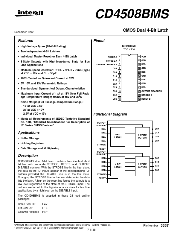
Functional Diagram
OUTPUT DISABLE D0A Q0A 4-BIT LATCH Q1A 3-STATE OUTUTS Q2A Q3A
Applications
- Buffer Storage
- Holding Registers
- Data Storage and Multiplexing
D1A D2A D3A STROBE RESET OUTPUT DISABLE D0B D1B D2B D3B STROBE RESET
Description
CD4508BMS...