CD4502BMS
Features
- High Voltage Type (20V Rating)
- 2 TTL Load Output Drive Capability
- 3 State Outputs
- mon Output Disable Control
- Inhibit Control
- 100% Tested for Quiescent Current at 20V
- 5V, 10V and 15V Parametric Ratings
- Maximum Input Current of 1µA at 18V Over Full Package Temperature Range; 100n A at 18V and +25o C
- Noise Margin (Over Full Package/Temperature Range)
- 1V at VDD = 5V
- 2V at VDD = 10V
- 2.5V at VDD = 15V
- Meets All Requirements of JEDEC Tentative Standard No. 13B, “Standard Specifications for Description of ‘B’ Series CMOS Devices”
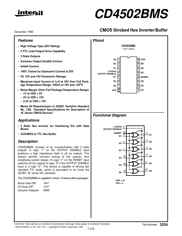
D3 Q3 D1
1 2 3
16 VDD 15 D6 14 Q6 13 D5 12 INHIBIT 11 Q5 10 D4 9 Q4
3 STATE 4 OUTPUT DISABLE Q1 5 D2 Q2 VSS 6 7 8
Functional Diagram
3 STATE 4 OUTPUT DISABLE 12 INHIBIT 3 D1 D2 6
Applications
- 3 State Hex Inverter for Interfacing ICs with Data Buses
- COS/MOS to TTL Hex Buffer
5 7
Q1 Q2
Description
CD4502BMS consists of six inverter/buffers with 3 state outputs. A logic “1” on the OUTPUT DISABLE input produces a high...