CD4006BMS
Features
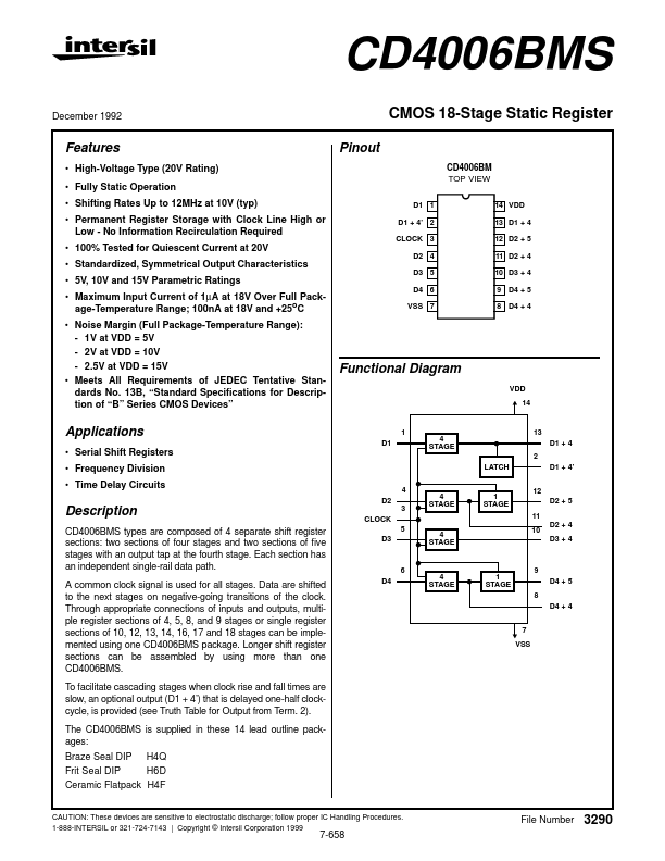
Pinout
- High-Voltage Type (20V Rating)
- Fully Static Operation
- Shifting Rates Up to 12MHz at 10V (typ)
- Permanent Register Storage with Clock Line High or Low
- No Information Recirculation Required
- 100% Tested for Quiescent Current at 20V
- Standardized, Symmetrical Output Characteristics
- 5V, 10V and 15V Parametric Ratings
- Maximum Input Current of 1µA at 18V Over Full Pack- age-Temperature Range; 100n A at 18V and +25o C
- Noise Margin (Full Package-Temperature Range):
- 1V at VDD = 5V
- 2V at VDD = 10V
- 2.5V at VDD = 15V
- Meets All Requirements of JEDEC Tentative Standards No. 13B, “Standard Specifications for Description of “B” Series CMOS Devices”
CD4006BM TOP VIEW
D1 1 D1 + 4’ 2 CLOCK 3
D2 4 D3 5 D4 6 VSS 7
14 VDD 13 D1 + 4 12 D2 + 5 11 D2 + 4 10 D3 + 4 9 D4 + 5 8 D4 + 4
Functional Diagram
VDD 14
Applications
- Serial Shift Registers
- Frequency Division
-...