Description
achieve the lowest on-state resistance in a package that has a footprint smaller than a D2PAK and only 0.7 mm profile.
Features
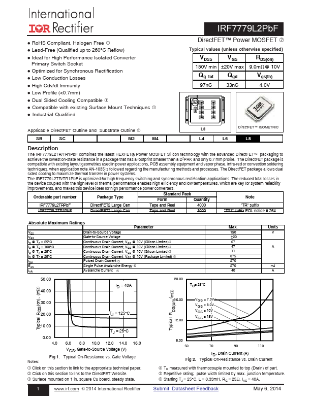
- l Gate Charge (nC)
Fig 8. Typical Capacitance vs. Drain-to-Source Voltage
Fig 9. Typical Total Gate Charge vs Gate-to-Source Voltage
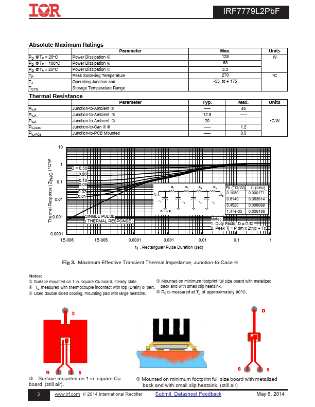
4
www. irf. com © 2014 International Rectifier
Submit Datasheet Feedback
May 6, 2014
IRF7779L2PbF
ISD, Reverse Drain Current (A)
ID , Drain Current (A) EAS, Single Pulse Avalanche Energy (mJ)
1000
100
TJ = 175°C TJ = 25°C
TJ = -40°C
10
1
VGS = 0V 0.1
0.2 0.4 0.6 0.8 1.0 VSD, Source-to-Drain Voltage (V)
Fig 10. Typical Source-Drain Diode Forward Voltage.
 IRF7779L2PBF Datasheet