Click to expand full text
1-MBIT (128K x 8) BOOT BLOCK FLASH MEMORY
28F001BX-T 28F001BX-B 28F001BN-T 28F001BN-B
Y
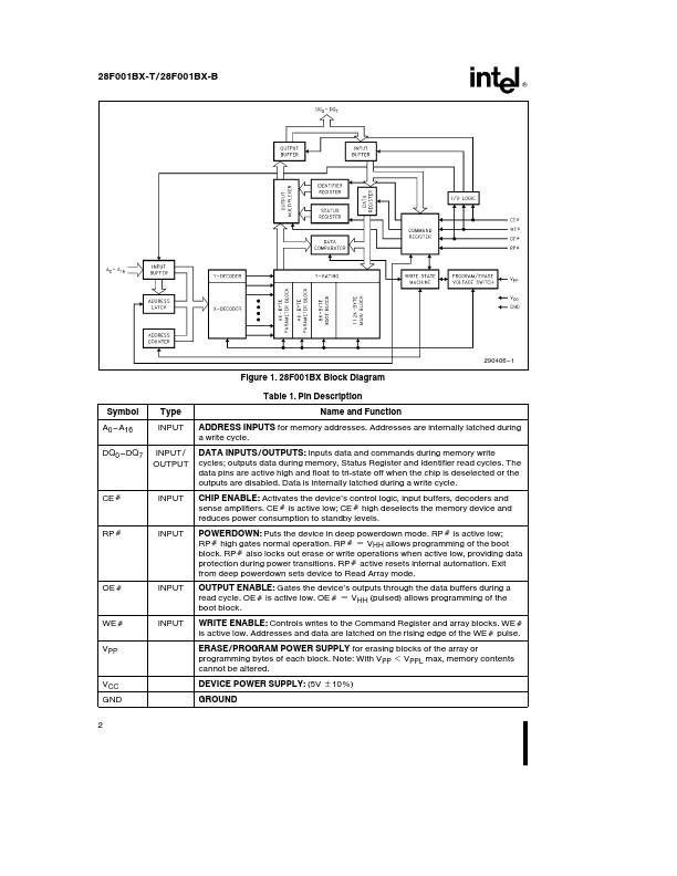
High-Integration Blocked Architecture One 8 KB Boot Block w Lock Out Two 4 KB Parameter Blocks One 112 KB Main Block 100 000 Erase Program Cycles Per Block Simplified Program and Erase Automated Algorithms via On-Chip Write State Machine (WSM) SRAM-Compatible Write Interface Deep Power-Down Mode 0 05 mA ICC Typical 0 8 mA IPP Typical 12 0V g 5% VPP
Y
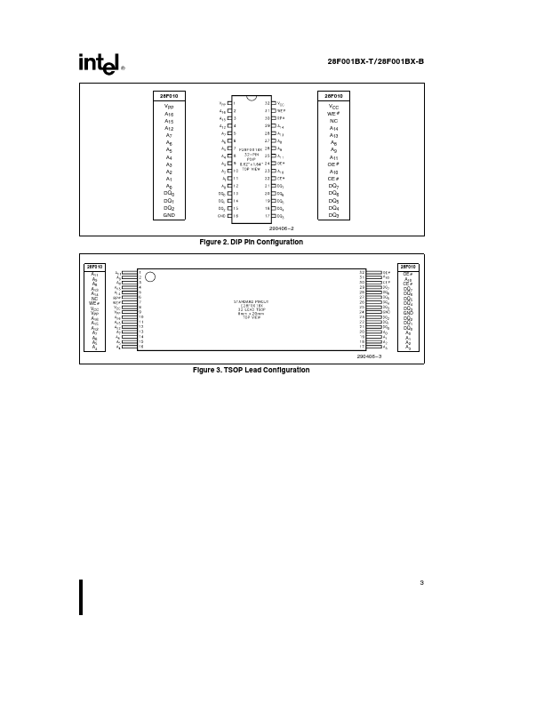
High-Performance Read 70 75 ns 90 ns 120 ns 150 ns Maximum Access Time 5 0V g 10% VCC Hardware Data Protection Feature Erase Write Lockout during Power Transitions Advanced Packaging JEDEC Pinouts 32-Pin PDIP 32-Lead PLCC TSOP ETOX TM II Nonvolatile Flash Technology EPROM-Compatible Process Base High-Volume Manufacturing Experience Extended Temperature O
 28F001BX-T Datasheet