Click to expand full text
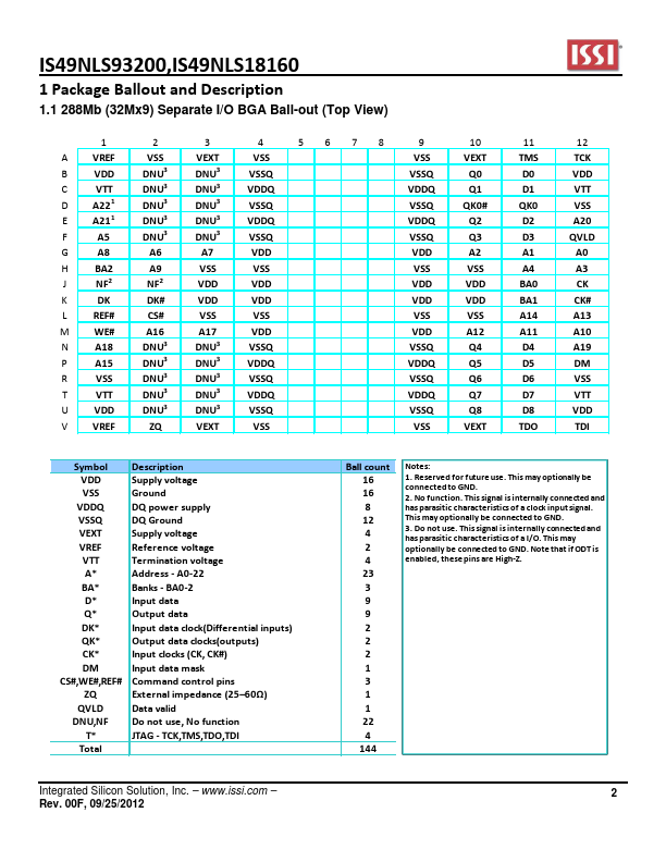
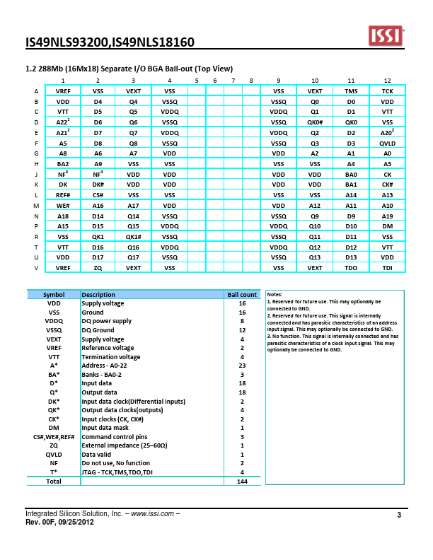
IS49NLS93200,IS49NLS18160
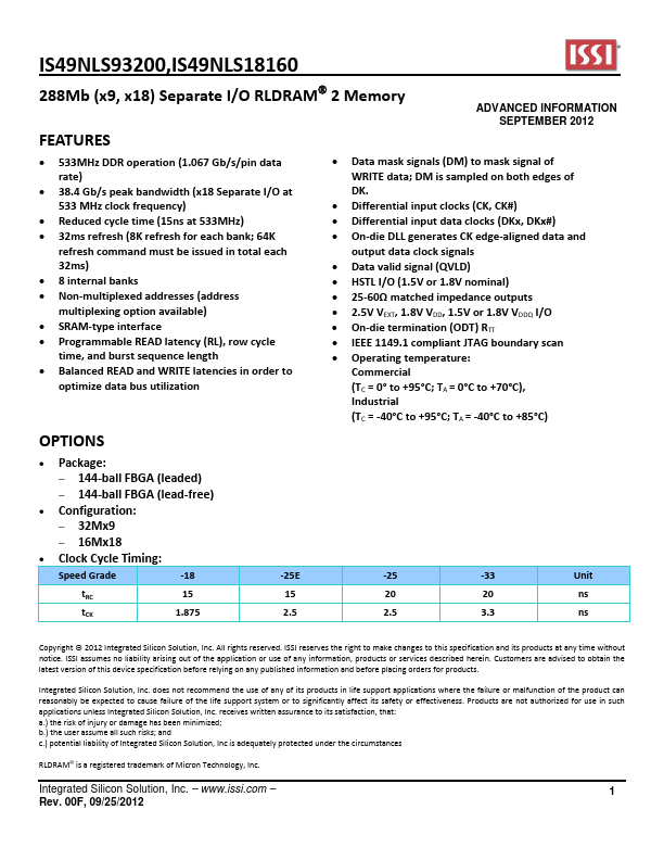
288Mb (x9, x18) Separate I/O RLDRAM® 2 Memory FEATURES
ADVANCED INFORMATION SEPTEMBER 2012
• 533MHz DDR operation (1.067 Gb/s/pin data rate)
• 38.4 Gb/s peak bandwidth (x18 Separate I/O at 533 MHz clock frequency)
• Reduced cycle time (15ns at 533MHz) • 32ms refresh (8K refresh for each bank; 64K
refresh command must be issued in total each 32ms) • 8 internal banks • Non-multiplexed addresses (address multiplexing option available) • SRAM-type interface • Programmable READ latency (RL), row cycle time, and burst sequence length • Balanced READ and WRITE latencies in order to optimize data bus utilization
• Data mask signals (DM) to mask signal of WRITE data; DM is sampled on both edges of DK.
 IS49NLS18160 Datasheet