Datasheet4U Logo Datasheet4U.com

IS49NLC96400 - Common I/O RLDRAM 2 Memory

Datasheet Summary

Description

1.1 576Mb (64Mx9) Common I/O BGA Ball‐out (Top View)  1 A VREF B VDD C VTT D A221 E A21 F A5 G A8 H BA2 J NF2 K DK L REF# M WE# N A18 P A15 R VSS T VTT U VDD V VREF 2 VSS DNU3 DNU3 DNU3 DNU3 DNU3 A6 A9 NF2 DK# CS# A16 DNU3 DNU3 DNU3 DNU3 DNU3 ZQ 3 VEXT DNU3 DNU3 DNU3 DNU3 DNU3 A7 VSS VDD VDD VSS

📥 Download Datasheet

Datasheet preview – IS49NLC96400

Datasheet Details

Part number IS49NLC96400
Manufacturer Integrated Silicon Solution
File Size 633.13 KB
Description Common I/O RLDRAM 2 Memory
Datasheet download datasheet IS49NLC96400 Datasheet
Additional preview pages of the IS49NLC96400 datasheet.
Other Datasheets by Integrated Silicon Solution

Full PDF Text Transcription

Click to expand full text
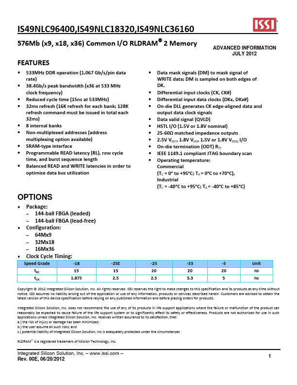
IS49NLC96400,IS49NLC18320,IS49NLC36160 576Mb (x9, x18, x36) Common I/O RLDRAM 2 Memory    FEATURES ADVANCED INFORMATION JULY 2012  533MHz DDR operation (1.067 Gb/s/pin data  rate)   38.4Gb/s peak bandwidth (x36 at 533 MHz  clock frequency)   Reduced cycle time (15ns at 533MHz)   32ms refresh (16K refresh for each bank; 128K  refresh command must be issued in total each  32ms)   8 internal banks   Non‐multiplexed addresses (address  multiplexing option available)   SRAM‐type interface   Programmable READ latency (RL), row cycle  time, and burst sequence length   Balanced READ and WRITE latencies in order to  optimize data bus utilization   Data mask signals (DM) to mask signal of  WRITE data; DM is sampled on both edges of  DK.
Published: |