Click to expand full text
IDT5V2528/A 2.5 / 3.3V PHASE-LOCK LOOP CLOCK DRIVER
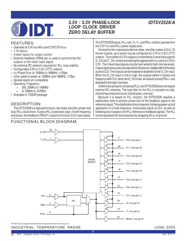
2.5V / 3.3V PHASE-LOCK LOOP CLOCK DRIVER ZERO DELAY BUFFER
INDUSTRIALTEMPERATURERANGE
IDT5V2528/A
FEATURES:
• Operates at 3.3V VDD/AVDD and 2.5V/3.3V VDDQ • 1:10 fanout • 3-level inputs for output control • External feedback (FBIN) pin is used to synchronize the
outputs to the clock input signal • No external RC network required for PLL loop stability • Configurable 2.5V or 3.3V LVTTL outputs • tPD Phase Error at 100MHz to 166MHz: ±150ps • Jitter (peak-to-peak) at 133MHz and 166MHz: ±75ps • Spread spectrum compatible • Operating Frequency:
− Std: 25MHz to 140MHz − A: 25MHz to 167MHz • Available in TSSOP package
DESCRIPTION:
The IDT5V2528 is a high performance, low-skew, low-jitter, phase-lock loop (PLL) clock driver.
 IDT5V2528A Datasheet