Datasheet Details
| Part number | IDT74FCT3932-100 |
|---|---|
| Manufacturer | Integrated Device Technology |
| File Size | 131.26 KB |
| Description | 3.3V LOW SKEW PLL-BASED CMOS CLOCK DRIVER |
| Datasheet |
 IDT74FCT3932-100 Datasheet IDT74FCT3932-100 Datasheet
|
|
|
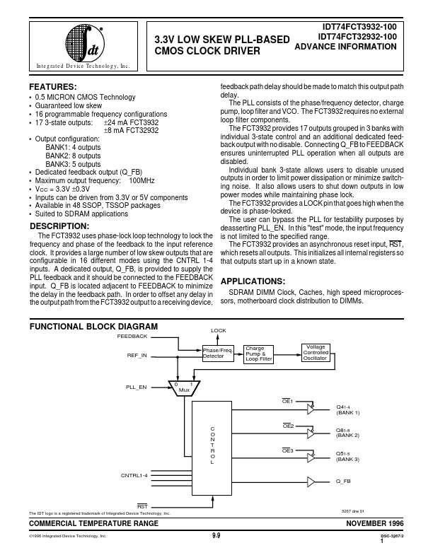
The FCT3932 uses phase-lock loop technology to lock the frequency and phase of the feedback to the input reference clock.
It provides a large number of low skew outputs that are configurable in 16 different modes using the CNTRL 1-4 inputs.
| Part number | IDT74FCT3932-100 |
|---|---|
| Manufacturer | Integrated Device Technology |
| File Size | 131.26 KB |
| Description | 3.3V LOW SKEW PLL-BASED CMOS CLOCK DRIVER |
| Datasheet |
IDT74FCT3932-100 Datasheet
|
|
|
|
| Part Number | Description | Manufacturer |
|---|---|---|
| IDT74FCT3244 | 3.3V CMOS OCTAL BUFFER/LINE DRIVER | Integrated Device Tech |
| IDT74FCT3244A | 3.3V CMOS OCTAL BUFFER/LINE DRIVER | Integrated Device Tech |
| IDT74FCT3245 | 3.3V CMOS OCTAL BIDIRECTIONAL TRANSCEIVERS | Integrated Device Tech |
| IDT74FCT3245 | 3.3V CMOS OCTAL BIDIRECTIONAL TRANSCEIVER | Renesas |
| IDT74FCT3245A | 3.3V CMOS OCTAL BIDIRECTIONAL TRANSCEIVERS | Integrated Device Tech |
| Part Number | Description |
|---|---|
| IDT74FCT3907 | 3.3V PENTIUM CLOCK SYNTHESIZER |
| IDT74FCT3807 | 3.3V CMOS 1-TO-10 CLOCK DRIVER |
| IDT74FCT3807A | 3.3V CMOS 1-TO-10 CLOCK DRIVER |
| IDT74FCT3827A | 3.3V CMOS 10-BIT BUFFERS |
| IDT74FCT3827B | 3.3V CMOS 10-BIT BUFFERS |
The following content is an automatically extracted verbatim text from the original manufacturer datasheet and is provided for reference purposes only.