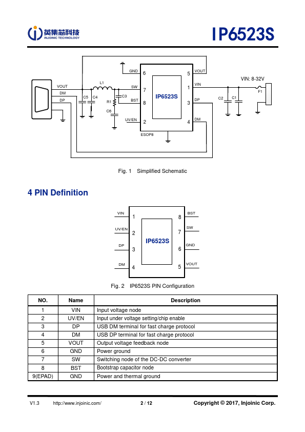
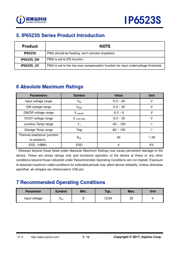
Input voltage node Input under voltage setting/chip enable USB DM terminal for fast charge protocol USB DP terminal for fast charge protocol Output voltage feedback node Power ground Switching node of the DC-DC converter Bootstrap capacitor node Power and thermal ground
V1.3
http://www.injoinic.co
Full PDF Text Transcription for IP6523S (Reference)
Note: Below is a high-fidelity text extraction (approx. 800 characters) for
IP6523S. For precise diagrams, tables, and layout, please refer to the original PDF.
IP6523S 3.4A OUTPUT STEP-DOWN CONVERTER with DCP PROTOCOLS 1 Features Synchronous step-down converter Built-in Power MOSFETs Wide Input Voltage Range, 8V to 32V O...
View more extracted text
ter Built-in Power MOSFETs Wide Input Voltage Range, 8V to 32V Output Voltage Range, 5V Max. Output Current, 3.4A Input Line Loss Compensation Output Current Limit Protection Conversion efficiency up to 96% Soft-Start Output Voltage Line Loss Compensation, 100mV@1A Supports DCP(BC1.
 IP6523S Datasheet