The following content is an automatically extracted verbatim text
from the original manufacturer datasheet and is provided for reference purposes only.
View original datasheet text
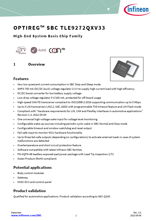
OPTIREG™ SBC TLE9272QXV33
High-End System Basis Chip Family
1
Overview
Features
• Very low quiescent current consumption in SBC Stop and Sleep mode • SMPS 750 mA (DC/DC buck) voltage regulator 3.3 V to supply high current load with high efficiency • DC/DC boost converter for low battery supply voltage • Low-drop voltage regulator 5 V/100 mA, protected for off-board usage • High-speed CAN FD transceiver compliant to ISO11898-2:2016 supporting communication up to 5 Mbps • Up to 3 LIN transceivers LIN2.2, SAE J2602 with programmable TXD timeout feature and LIN Flash mode • Compliant with “Hardware requirements for LIN, CAN and FlexRay interfaces in automotive applications”
Revision 1.
 TLE9272QXV33 Datasheet