Click to expand full text
s
OptiMOSTM3 Power-Transistor
Package Marking • N-channel, normal level • Excellent gate charge x R DS(on) product (FOM) • Very low on-resistance R DS(on) • 150 °C operating temperature • Pb-free lead plating; RoHS compliant • Qualified according to JEDEC1) for target application • Halogen-free according to IEC61249-2-21
BSZ900N15NS3 G
Product Summary V DS R DS(on),max ID
150 V 90 mΩ 13 A
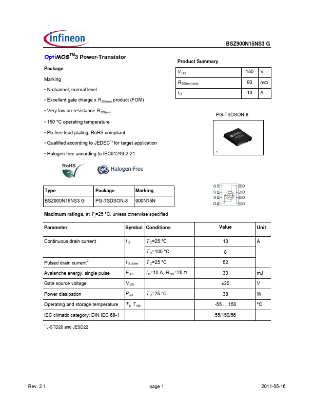
PG-TSDSON-8
Type BSZ900N15NS3 G
Package PG-TSDSON-8
Marking 900N15N
Maximum ratings, at T j=25 °C, unless otherwise specified
Parameter
Symbol Conditions
Continuous drain current
I D T C=25 °C
T C=100 °C
Pulsed drain current2)
I D,pulse T C=25 °C
Avalanche energy, single pulse
E AS I D=10 A, R GS=25 Ω
Gate source voltage
V GS
Power dissipation
P tot T C=25 °C
Operating and storage te
 900N15N Datasheet