Datasheet4U Logo Datasheet4U.com

IS61VF102418A - (IS61xFxxxxxA) Synchronous Flow-through Static RAM

This page provides the datasheet information for the IS61VF102418A, a member of the IS61LF25672A (IS61xFxxxxxA) Synchronous Flow-through Static RAM family.

Datasheet Summary

Description

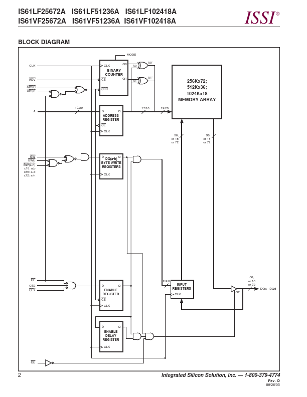
IS61LF/VF102418A are high-speed, low-power synchronous static RAMs designed to provide burstable, highperformance memory for communication and networking applications.

The IS61LF/VF25672A is organized as 262,144 words by 72 bits.

Features

  • Internal self-timed write cycle.
  • Individual Byte Write Control and Global Write.
  • Clock controlled, registered address, data and control.
  • Burst sequence control using MODE input.
  • Three chip enable option for simple depth expansion and address pipelining.
  • Common data inputs and data outputs.
  • Auto Power-down during deselect.
  • Single cycle deselect.
  • Snooze MODE for reduced-power standby.
  • JTAG Boundary Scan for.

📥 Download Datasheet

Datasheet preview – IS61VF102418A

Datasheet Details

Part number IS61VF102418A
Manufacturer ISSI
File Size 309.96 KB
Description (IS61xFxxxxxA) Synchronous Flow-through Static RAM
Datasheet download datasheet IS61VF102418A Datasheet
Additional preview pages of the IS61VF102418A datasheet.
Other Datasheets by ISSI

Full PDF Text Transcription

Click to expand full text
( DataSheet : www.DataSheet4U.com ) IS61LF25672A IS61VF25672A IS61LF51236A IS61VF51236A IS61LF102418A IS61VF102418A 256K x 72, 512K x 36, 1024K x 18 18Mb SYNCHRONOUS FLOW-THROUGH STATIC RAM ISSI AUGUST 2005 ® FEATURES • Internal self-timed write cycle • Individual Byte Write Control and Global Write • Clock controlled, registered address, data and control • Burst sequence control using MODE input • Three chip enable option for simple depth expansion and address pipelining • Common data inputs and data outputs • Auto Power-down during deselect • Single cycle deselect • Snooze MODE for reduced-power standby • JTAG Boundary Scan for PBGA package • Power Supply LF: VDD 3.3V + 5%, VDDQ 3.3V/2.5V + 5% VF: VDD 2.5V + 5%, VDDQ 2.
Published: |