Datasheet4U Logo Datasheet4U.com

IS46DR81280C - DDR2 DRAM

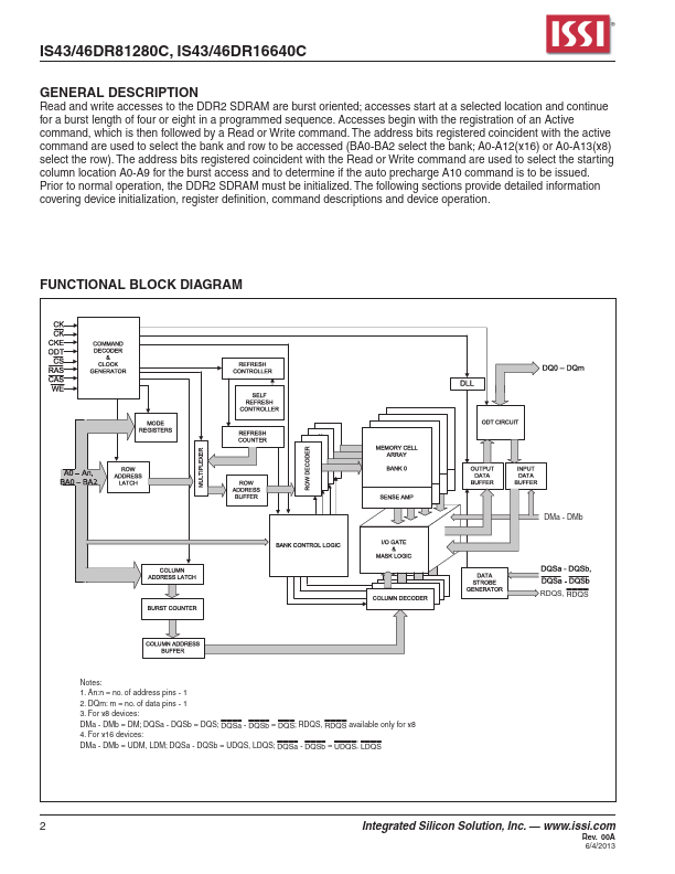
This page provides the datasheet information for the IS46DR81280C, a member of the IS43DR81280C DDR2 DRAM family.

Datasheet Summary

Description

architecture to achieve high-speed operation.

data words per clock cycle at the I/O balls.

Features

  • Vdd = 1.8V ±0.1V, Vddq = 1.8V ±0.1V.
  • JEDEC standard 1.8V I/O (SSTL_18-compatible).
  • Double data rate interface: two data transfers per clock cycle.
  • Differential data strobe (DQS, DQS).
  • 4-bit prefetch architecture.
  • On chip DLL to align DQ and DQS transitions with CK.
  • 8 internal banks for concurrent operation.
  • Programmable CAS latency (CL) 3, 4, 5, 6 and 7 supported.
  • Posted CAS and programmable additive laten.

📥 Download Datasheet

Datasheet preview – IS46DR81280C

Datasheet Details

Part number IS46DR81280C
Manufacturer ISSI
File Size 872.14 KB
Description DDR2 DRAM
Datasheet download datasheet IS46DR81280C Datasheet
Additional preview pages of the IS46DR81280C datasheet.
Other Datasheets by ISSI

Full PDF Text Transcription

Click to expand full text
IS43/46DR81280C IS43/46DR16640C 128Mx8, 64Mx16 DDR2 DRAM FEATURES • Vdd = 1.8V ±0.1V, Vddq = 1.8V ±0.1V • JEDEC standard 1.
Published: |