Datasheet4U Logo Datasheet4U.com

IS43TR81280B - 1Gb DDR3 SDRAM

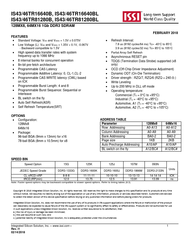
This page provides the datasheet information for the IS43TR81280B, a member of the IS43TR16640B 1Gb DDR3 SDRAM family.
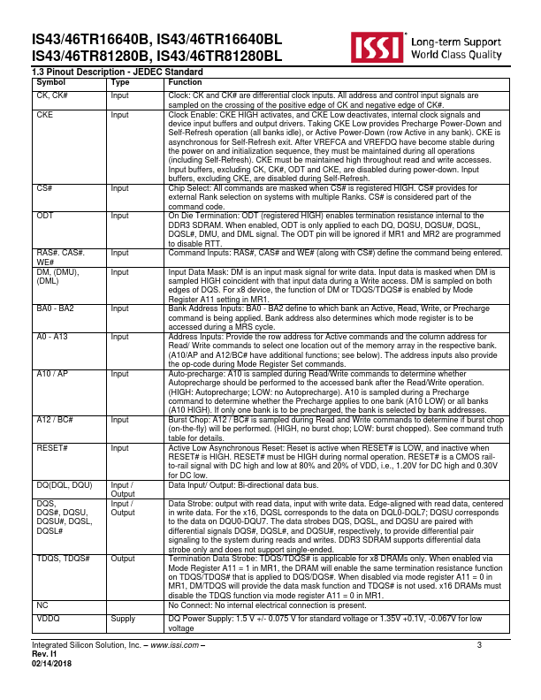
Datasheet Summary

Description

CS# ODT RAS#.

CAS#.

Clock: CK and CK# are differential clock inputs.

Features

  • Standard Voltage: VDD and VDDQ = 1.5V ± 0.075V.
  • Low Voltage (L): VDD and VDDQ = 1.35V + 0.1V, -0.067V - Backward compatible to 1.5V.
  • High speed data transfer rates with system frequency up to 1066 MHz.
  • 8 internal banks for concurrent operation.
  • 8n-bit pre-fetch architecture.
  • Programmable CAS Latency.
  • Programmable Additive Latency: 0, CL-1,CL-2.
  • Programmable CAS WRITE latency (CWL) based on tCK.
  • Programmable Burst Length: 4 and 8.
  • Programmable Bu.

📥 Download Datasheet

Datasheet preview – IS43TR81280B

Datasheet Details

Part number IS43TR81280B
Manufacturer ISSI
File Size 3.11 MB
Description 1Gb DDR3 SDRAM
Datasheet download datasheet IS43TR81280B Datasheet
Additional preview pages of the IS43TR81280B datasheet.
Other Datasheets by ISSI

Full PDF Text Transcription

Click to expand full text
IS43/46TR16640B, IS43/46TR16640BL IS43/46TR81280B, IS43/46TR81280BL 128MX8, 64MX16 1Gb DDR3 SDRAM FEATURES  Standard Voltage: VDD and VDDQ = 1.5V ± 0.075V  Low Voltage (L): VDD and VDDQ = 1.35V + 0.1V, -0.067V - Backward compatible to 1.5V  High speed data transfer rates with system frequency up to 1066 MHz  8 internal banks for concurrent operation  8n-bit pre-fetch architecture  Programmable CAS Latency  Programmable Additive Latency: 0, CL-1,CL-2  Programmable CAS WRITE latency (CWL) based on tCK  Programmable Burst Length: 4 and 8  Programmable Burst Sequence: Sequential or Interleave  BL switch on the fly  Auto Self Refresh(ASR)  Self Refresh Temperature(SRT) OPTIONS  Configuration: 128Mx8 64Mx16  Package: 96-ball FBGA (9mm x 13mm) for x16 78-ball FBGA (8mm x 10.
Published: |