Datasheet4U Logo Datasheet4U.com

IS43LR16640A - 16M x 16Bits x 4Banks Mobile DDR SDRAM

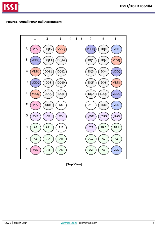
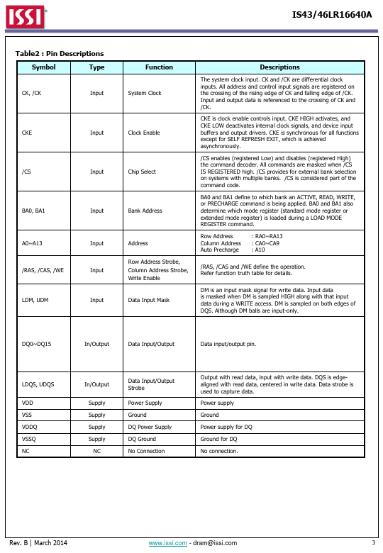
This page provides the datasheet information for the IS43LR16640A, a member of the IS46LR16640A 16M x 16Bits x 4Banks Mobile DDR SDRAM family.

Datasheet Summary

Description

The IS43/46LR16640A is 1,073,741,824 bits CMOS Mobile Double Data Rate Synchronous DRAM organized as 4 banks of 16,777,216 words x 16 bits.

This product uses a double-data-rate architecture to achieve high-speed operation.

The Data Input/ Output signals are transmitted on a 16-bit bus.

Features

  • JEDEC standard 1.8V power supply.
  • VDD = 1.8V, VDDQ = 1.8V.
  • Four internal banks for concurrent operation.
  • MRS cycle with address key programs - CAS latency 2, 3 (clock) - Burst length (2, 4, 8) - Burst type (sequential & interleave).
  • Fully differential clock inputs (CK, /CK).
  • All inputs except data & DM are sampled at the rising edge of the system clock.
  • Data I/O transaction on both edges of data strobe.
  • Bidirectional data.

📥 Download Datasheet

Datasheet preview – IS43LR16640A

Datasheet Details

Part number IS43LR16640A
Manufacturer ISSI
File Size 1.16 MB
Description 16M x 16Bits x 4Banks Mobile DDR SDRAM
Datasheet download datasheet IS43LR16640A Datasheet
Additional preview pages of the IS43LR16640A datasheet.
Other Datasheets by ISSI

Full PDF Text Transcription

Click to expand full text
IS43/46LR16640A 16M x 16Bits x 4Banks Mobile DDR SDRAM Description The IS43/46LR16640A is 1,073,741,824 bits CMOS Mobile Double Data Rate Synchronous DRAM organized as 4 banks of 16,777,216 words x 16 bits. This product uses a double-data-rate architecture to achieve high-speed operation. The Data Input/ Output signals are transmitted on a 16-bit bus. The double data rate architecture is essentially a 2N prefetch architecture with an interface designed to transfer two data words per clock cycle at the I/O pins. This product offers fully synchronous operations referenced to both rising and falling edges of the clock. The data paths are internally pipelined and 2n-bits prefetched to achieve very high bandwidth. All input and output voltage levels are compatible with LVCMOS.
Published: |