Datasheet4U Logo Datasheet4U.com

IS43DR16640B - 1Gb DDR2 SDRAM

This page provides the datasheet information for the IS43DR16640B, a member of the IS46DR81280B 1Gb DDR2 SDRAM family.

Datasheet Summary

Description

DDR2 SDRAM (128Mx8) TW-BGA Ball-out (Top-View) (8.00mm x 10.50mm) Symbol CK, CK# CKE CS# RAS#,CAS#,WE# A[13:0] BA[2:0] DQ[7:0] DQS, DQS# RDQS, RDQS# DM VDD VSS VDDQ VSSQ VREF VDDL VSSDL ODT NC Description Input clocks Clock enable Chip Select Command control pins Address Bank Address I/O Data Stro

Features

  • Clock frequency up to 400MHz.
  • 8 internal banks for concurrent operation.
  • 4-bit prefetch architecture.
  • Programmable CAS Latency: 3, 4, 5, 6 and 7.
  • Programmable Additive Latency: 0, 1, 2, 3, 4, 5 and 6.
  • Write Latency = Read Latency-1.
  • Programmable Burst Sequence: Sequential or Interleave.
  • Programmable Burst Length: 4 and 8.
  • Automatic and Controlled Precharge Command.
  • Power Down Mode.
  • Auto Refresh and Self Refresh.
  • Refresh Interval: 7.8 .

📥 Download Datasheet

Datasheet preview – IS43DR16640B

Datasheet Details

Part number IS43DR16640B
Manufacturer ISSI
File Size 1.04 MB
Description 1Gb DDR2 SDRAM
Datasheet download datasheet IS43DR16640B Datasheet
Additional preview pages of the IS43DR16640B datasheet.
Other Datasheets by ISSI

Full PDF Text Transcription

Click to expand full text
IS43/46DR81280B(L), IS43/46DR16640B(L) 
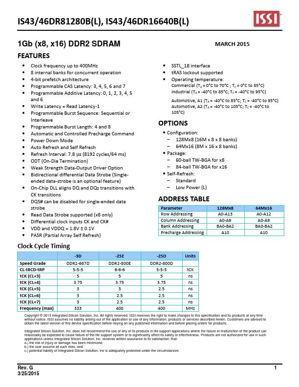
1Gb (x8, x16) DDR2 SDRAM MARCH 2015 FEATURES  Clock frequency up to 400MHz  8 internal banks for concurrent operation  4-bit prefetch architecture  Programmable CAS Latency: 3, 4, 5, 6 and 7  Programmable Additive Latency: 0, 1, 2, 3, 4, 5 and 6  Write Latency = Read Latency-1  Programmable Burst Sequence: Sequential or Interleave  Programmable Burst Length: 4 and 8  Automatic and Controlled Precharge Command  Power Down Mode  Auto Refresh and Self Refresh  Refresh Interval: 7.
Published: |