Datasheet4U Logo Datasheet4U.com

IS42VM16200D - 1M x 16Bits x 2Banks Low Power Synchronous DRAM

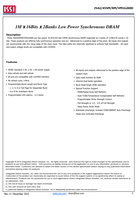
This page provides the datasheet information for the IS42VM16200D, a member of the IS42SM16200D 1M x 16Bits x 2Banks Low Power Synchronous DRAM family.

Datasheet Summary

Description

These IS42SM/RM/VM16200D are low power 33,554,432 bits CMOS Synchronous DRAM organized as 2 banks of 1,048,576 words x 16 bits.

These products are offering fully synchronous operation and are referenced to a positive edge of the clock.

Features

  • JEDEC standard 3.3V, 2.5V, 1.8V power supply.
  • Auto refresh and self refresh.
  • All pins are compatible with LVCMOS interface.
  • 4K refresh cycle / 64ms.
  • Programmable Burst Length and Burst Type - 1, 2, 4, 8 or Full Page for Sequential Burst - 4 or 8 for Interleave Burst.
  • Programmable CAS Latency : 2,3 clocks.
  • All inputs and outputs referenced to the positive edge of the system clock.
  • Data mask function by DQM.
  • Internal du.

📥 Download Datasheet

Datasheet preview – IS42VM16200D

Datasheet Details

Part number IS42VM16200D
Manufacturer ISSI
File Size 517.44 KB
Description 1M x 16Bits x 2Banks Low Power Synchronous DRAM
Datasheet download datasheet IS42VM16200D Datasheet
Additional preview pages of the IS42VM16200D datasheet.
Other Datasheets by ISSI

Full PDF Text Transcription

Click to expand full text
IS42/45SM/RM/VM16200D 1M x 16Bits x 2Banks Low Power Synchronous DRAM Description These IS42SM/RM/VM16200D are low power 33,554,432 bits CMOS Synchronous DRAM organized as 2 banks of 1,048,576 words x 16 bits. These products are offering fully synchronous operation and are referenced to a positive edge of the clock. All inputs and outputs are synchronized with the rising edge of the clock input. The data paths are internally pipelined to achieve high bandwidth. All input and output voltage levels are compatible with LVCMOS. Features  JEDEC standard 3.3V, 2.5V, 1.
Published: |