Full PDF Text Transcription for TK6P65W (Reference)
Note: Below is a high-fidelity text extraction (approx. 800 characters) for
TK6P65W. For precise diagrams, and layout, please refer to the original PDF.
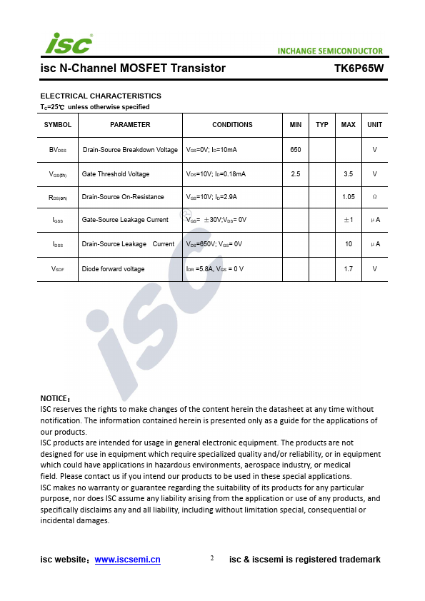
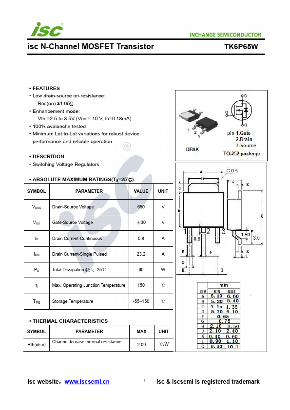
Enhancement mode: Vth =2.5 to 3.5V (VDS = 10 V, ID=0.18mA) ·100% avalanche tested ·Minimum Lot-to-Lot variations for robust device performance and reliable operation ·DESCRITION ·Switching Voltage Regulators ·ABSOLUTE MAXIMUM RATINGS(Ta=25℃) SYMBOL PARAMETER VALUE UNIT VDSS Drain-Source Voltage 650 V VGS Gate-Source Voltage ±30 V ID Drain Current-Continuous 5.8 A IDM Drain Current-Single Pulsed 23.2 A PD Total Dissipation @TC=25℃ 60 W Tj Max. Operating Junction Temperature 150 ℃ Tstg Storage Temperature -55~150 ℃ ·THERMAL CHARACTERISTICS SYMBOL PARAMETER Rth(ch-c) Channel-to-case thermal resistance MAX 2.09 UNIT ℃/W isc we
 TK6P65W Datasheet