Datasheet Details
| Part number | STW25NM60ND |
|---|---|
| Manufacturer | Inchange Semiconductor |
| File Size | 349.27 KB |
| Description | N-Channel MOSFET |
| Datasheet |
 STW25NM60ND Datasheet STW25NM60ND Datasheet
|
|
|
| Part number | STW25NM60ND |
|---|---|
| Manufacturer | Inchange Semiconductor |
| File Size | 349.27 KB |
| Description | N-Channel MOSFET |
| Datasheet |
STW25NM60ND Datasheet
|
|
|
|
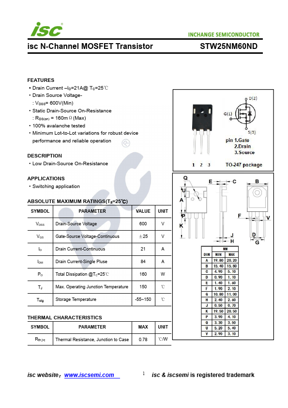
·Low Drain-Source On-Resistance APPLICATIONS ·Switching application ABSOLUTE MAXIMUM RATINGS(Ta=25℃) SYMBOL PARAMETER VALUE UNIT VDSS Drain-Source Voltage 600 V VGS Gate-Source Voltage-Continuous ±25 V ID Drain Current-Continuous 21 A IDM Drain Current-Single Pluse 84 A PD Total Dissipation @TC=25℃ 160 W TJ Max.
Operating Junction Temperature 150 ℃ Tstg Storage Temperature -55~150 ℃ THERMAL CHARACTERISTICS SYMBOL PARAMETER Rth j-c Thermal Resistance, Junction to Case MAX 0.78 UNIT ℃/W STW25NM60ND isc website:www.iscsemi.com 1 isc & iscsemi is registered trademark isc N-Channel MOSFET Transistor STW25NM60ND ELECTRICAL CHARACTERISTICS TC=25℃ unless otherwise specified SYMBOL PARAMETER CONDITIONS V(BR)DSS Drain-Source Breakdown Voltage VGS= 0;
ID= 1mA VGS(th) Gate Threshold Voltage VDS= VGS;
isc N-Channel MOSFET Transistor.
| Brand Logo | Part Number | Description | Manufacturer |
|---|---|---|---|
| STW25NM60ND | N-channel MOSFET | STMicroelectronics | |
| STW25NM60N | N-CHANNEL Power MOSFET | ST Microelectronics |
| Part Number | Description |
|---|---|
| STW20N65M5 | N-Channel MOSFET |
| STW20NM50FD | N-Channel MOSFET |
| STW20NM60 | N-Channel MOSFET |
| STW20NM60FD | N-Channel MOSFET |
| STW21N65M5 | N-Channel MOSFET |
| STW21NM60ND | N-Channel MOSFET |
| STW22NM60N | N-Channel MOSFET |
| STW23NM50N | N-Channel MOSFET |
| STW23NM60ND | N-Channel MOSFET |
| STW24NM60N | N-Channel MOSFET |