MDD1051RH
FEATURES
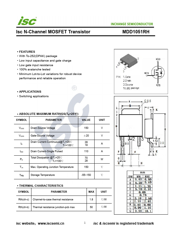
- With To-252(DPAK) package
- Low input capacitance and gate charge
- Low gate input resistance
- 100% avalanche tested
- Minimum Lot-to-Lot variations for robust device performance and reliable operation
- APPLICATIONS
- Switching applications
- ABSOLUTE MAXIMUM RATINGS(Ta=25℃)
SYMBOL
PARAMETER
VALUE
VDSS
Drain-Source Voltage
VGSS ID IDM PD Tch
Gate-Source Voltage
Drain Current-Continuous@TC=25℃ TC=100℃
Drain Current-Single Pulsed
Total Dissipation @TC=25℃ TC=100℃
Max. Operating Junction Temperature
±20
28 18
70 28
Tstg
Storage Temperature
-55~150
UNIT V V A A W ℃ ℃
- THERMAL CHARACTERISTICS
SYMBOL
PARAMETER
Rth(ch-c) Channel-to-case thermal resistance
Rth(ch-b) Thermal resistance junction-pcb max
MAX 1.8 50
UNIT ℃/W ℃/W isc website:.iscsemi.cn
1 isc & iscsemi is registered trademark
Isc N-Channel MOSFET Transistor
INCHANGE...